Wide-Bandgap Semis
Current
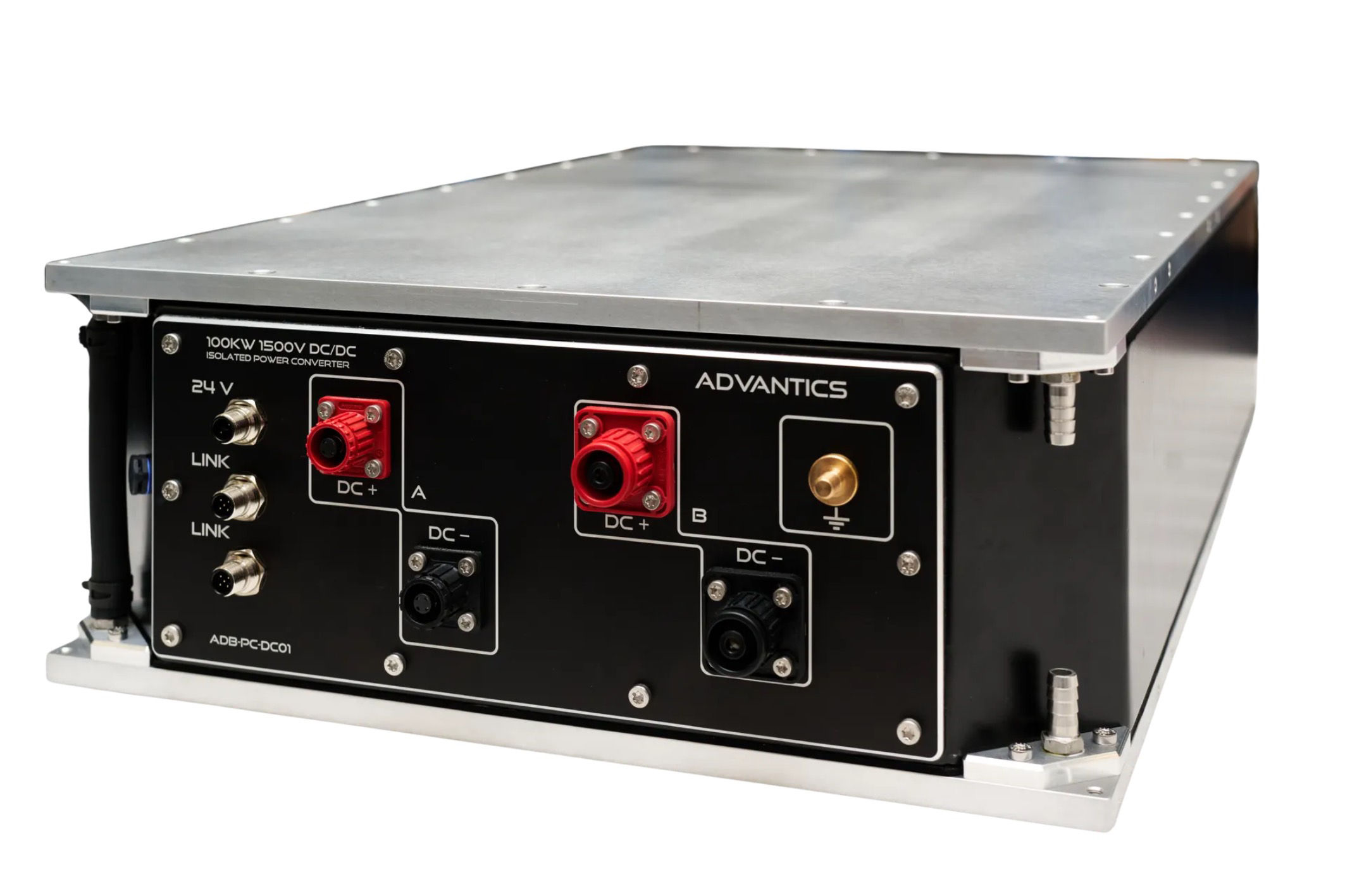
ADVANTICS’ liquid-cooled power conversion platform is based on modular 100 kW building blocks, enabling scalable systems up to the megawatt range.
Infineon Technologies AG will supply CoolSiC™ MOSFETs 1200 V and matching dual-channel EiceDRIVER™ 2EDB9259Y gate drivers to ADVANTICS, a technology leader in silicon carbide (SiC) power electronics and advanced control systems, for its new line of liquid-cooled power converters. The solutions enhance ef
. . . Learn More
Date:
07/08/2026
Archive