Author:
Nare Gabrielyan, Product Marketing Manager, Cambridge GaN Devices
Date
01/20/2025
 PDF
PDF

Click image to enlarge
Size, weight and performance are three attributes that constantly propel electronics development. Throw in the need for ultra-efficiency driven by market requirements and international regulations, plus the absolute need to address sustainability, and you’ll see why gallium nitride is gaining such huge traction as a power semiconductor technology.
In stark contrast to the overall semiconductor market, which fell about 8.2% in 2023, GaN power semiconductor revenues grew by 41%, according to a reportby specialist analyst company, Yole Group. That growth, continues the report, is set to continue at 45% in 2024, then accelerate to 65% in 2025. Yole, plus other analysts, set the CAGR for GaN power semiconductors to range anywhere from 30-50% running up to the end of the decade, and for the GaN power semiconductor to be worth anything up to $5B by 2032.
The reason why analyst figures vary so widely is that they can only be as accurate as the information they receive. The situation is changing so rapidly, with frequent announcements of new performance metrics which open up GaN to more applications, and investments in production capability – to say nothing of mergers, acquisitions, and, sadly, but predictably,litigation, that a prediction concerning GaN power market size going forward more than 18 months is likely to be inaccurate. This is always the case for a disruptive technology…with little history to base calculations upon and only a guesstimate of the total addressable market size, the work of analysts is far from easy.
Whatever the absolute numbers turn out to be, the indications are that GaN is already big and will become much, much bigger. Bullish commentators will even argue that GaN will likely replace silicon as the power semiconductor technology of choice, more or less completely, within 10-15 years. Why is this?
GaN is a More Efficient Switch
Simply put, a GaN switch (HEMT) is much closer to a ‘perfect’ switch than a silicon MOSFET, with almost lossless operation. Its FoM on multiple dimensions (Figure of Merit: a comparative performance measure) is 10 times better than silicon. This means that power converters can be made smaller and more efficient.
Ease of Manufacture and Use
Most GaN ICs are produced using traditional silicon wafers as a substrate. The GaN-on-Si wafers are processed using the same, or very similar processing techniques as traditional silicon devices, often in the same fabs. Happily, this is in complete contrast to other materials, such as silicon carbide, which need different equipment and very high temperatures. GaN ICs also require, in principle, fewer mask steps than superjunction MOSFETs.
If we turn to their use, although early GaN devices needed special design-in attention, newer devices, such as CGD’s ICeGaNGaN ICs, integrate a driver interface and protection circuitry as well as the power switch on the GaN chip, so designers can benefit from the power density and efficiency benefits of GaN without having to learn whole new design methodologies.
Room for Even More Improvement
Currently, GaN power ICs are enabling power supplies to be shrunk by as much as 50%, while operating at efficiency levels approaching and even exceeding 95%. This means that power supplies can easily comply with international efficiency regulations such as 80 plus Titanium.
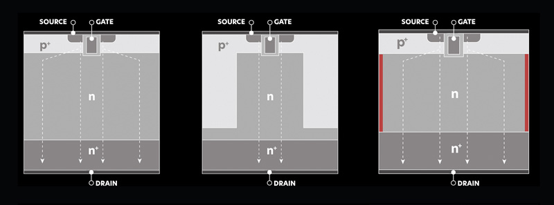
But, if you look at the FoM ratings released by GaN vendors you will notice that – unlike silicon or SiC – GaN devices are positioned 10 to 100 times inside the theoretical limit, in terms of specific resistance vs breakdown voltage. Therefore, we believe that there is much room for GaN devices to improve when considering chip dimensions and losses.
Basically, GaN is just at the start of its journey.
Sustainability
The world has woken up to the fact that the earth’s resources are limited and that we must reduce our carbon footprint for the sake of the health of the planet and all the life forms that inhabit it. Because it enables high-efficiency operation, GaN is a technology that can make a positive contribution to sustainability.
Cost
Currently, individual GaN ICs tend to carry a price premium over their silicon counterparts. However, if one considers system costs, using GaN makes it possible to reduce the required thermal management components, simplify the design, reducing BOM count, and shrink the size of the magnetic components required. Therefore, system costs using GaN may already be less than traditional silicon; in fact, this has already been demonstrated on a number of applications.Also, GaN IC production is scaling up massively, so GaN IC prices will inevitably continue to fall as 200mm wafers become the standard and, in the mid term, 300mm wafer capacity comes onstream.
A Disruptive Technology
Given these attributes, GaN is a highly disruptive technology. The task of the GaN industry now is to remove any misconceptions that somehow GaN is limited in the size of the chip, in the current that it can carry, and, therefore, in the application power levels that it can address. Some initial limitations when compared to Silicon Carbide (high current and high temperature capability) are being progressively addressed as new designs and technology nodes are reached. Then, of course, there will be no reasons why GaN can not be used for very high-power applications. It's just a matter of time.
We have already seen GaN transistors with RDS(on) values of just 10s of milliohms, enabling them to target applications up to a few kilowatts. Now we are seeing devices at just 10 milliohms, and the roadmap plans to go much lower. It's a matter of manufacturability and keeping production yields under control.
From a reliability standpoint, there are no specific roadblocks that will prevent GaN ICs from being employed in very demanding applications requiring more than 10 years of lifetime. This will require very low failure ppm rates, and this is also another direction the GaN industry is taking—that’s also CGD’s strategy. The basic idea of the ICeGaN concept is to make a self-protected chip, delivering a transistor that does not have any weaknesses.
Markets – Now and in the Near Future
If GaN develops as outlined above—and every indication is that it will—then all industry sectors will be impacted. Initially, GaN ICs found a market in USB-PD chargers for smart mobile devices at power levels of up to 100W. GaN was preferred for new-generation sleek, modern designs, and, indeed, the term ‘GaN’ has been used as a marketing labelto convey stylish design and small size.
The power of GaN chargers/adapters has now increased to more than 100W. This opens up many more applications, including laptops and notebooks, home appliances, and other consumer and industrial equipment. According to CGD’s business intelligence,the GaN-powered chargers market size is projected to grow from $0.2B in 2023 to more than $1B by 2032, at a CAGR of more than 20%.
Emobility is another sector that is now embracing GaN-based power chargers which are now available for e-bikes and e-scooters. When considering BEVs, although GaN is not yet to be found in the powertrain, GaN-based designs are gaining prominence for several automotive applications, such as On-Board Chargers and DC-DC conversion, driven by strong requirements for smaller form factor and reduced weight.
Artificial Intelligence (AI) gets a huge amount of press these days; one of the aspects of AI that is not always considered is the strain that high-performance GPUs put on data centres. Until very recently, a power rating of 15kW was the norm for a data centre rack. Now that figure is 100kW with 200kW expected soon. Delivering that amount of power efficiently and in the available space requires a complete reconsideration of the power system design, and GaN looks set to play an increasing role.

Click image to enlarge
Solar and wind inverters are yet another application that is in the late stages of designing power schemes around GaN. Still, genuinely, as fast as GaN can deliver higher and higher power levels, the market is set to adopt it as the technology of choice. Putting a figure on the number of GaN power supplies that will be in operation, even in the near future of just a few years, is impossible. We are living in the electronic age – which ironically has been termed the ‘Silicon Age’. Every aspect of our lives is reliant on electronic devices, equipment and systems. Everything electronic needs power and GaN is the most efficient way to deliver power. Welcome to the GaN Era, come join the fun.