Author:
Frederik Dostal, Power Management Expert, Analog Devices
Date
01/20/2025
 PDF
PDF

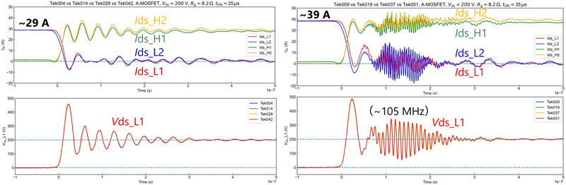
Figure 1. Necessary components to consider when using GaN technology as power switches in a power stage of the LTC7800 buck converter.
Click image to enlarge
GaN switches typically have lower gate voltage ratings than silicon FETs. Most GaN manufacturers recommend a typical gate drive voltage of 5 V. Some have an absolute maximum rating of 6 V, which does not give much headroom between the recommended gate drive voltage and the critical threshold, above which would damage the device. Recommended gate drives vary from manufacturer to manufacturer. This limitation, along with the fact that the gate charge in GaN devices is so small, means that driver stages must strictly limit the maximum gate drive voltage to avoid damage to the GaN device.
One must also deal with the fast voltage change (dv/dt) of the switch node of the power supply. This may cause false turn-on of the bottom switch. The gate of GaN devices is quite small. Any fast voltage changes in the vicinity, such as the switch node, may capacitively couple onto the small gate of the GaN switch and turn it on. To have more control of the turn-on and turn-off profiles, a separate pull-up and pull-down pin and a carefully designed printed circuit board layout are needed.
Lastly, GaN FETs have a higher conduction loss during dead times. These are the times when both the high-side and low-side switch of a bridge configuration are turned off. Dead times are necessary to prevent a short circuit from the high-side voltage rail to ground. During the dead time, typically, the low-side switch develops current flow through a body diode of the lowside switch. One way of solving this problem of high conduction losses during such dead times is to strictly minimize the length of these dead times without generating overlapping times of the high-side and low-side switches.
One other item to mention is the fact that GaN offers a wider conversion range. The fast rise and fall times provide smaller duty cycle than with silicon MOSFETs.
Replacing Silicon
Figure 1 shows a power stage of a typical buck regulator switch-mode power supply. The red arrows indicate additional components that may be necessary when using GaN switches in a switch-mode power supply. GaN switches do not offer the convenience of a body diode. The body diode in a silicon MOSFET is a p-n junction, which occurs by the structure of the silicon process. The process of GaN technology is somewhat different so a simple p-n junction body diode is not available. However, GaN switches have a different mechanism to yield similar results. Only majority carriers are involved in GaN device conduction so there is zero reverse recovery. However, the GaN FET does not have the forward voltage of the body diode, as with silicon MOSFETs, so the voltage across the GaN FET may get quite large. Thus, the power losses during the dead time are quite high. This is the reason for the importance of reducing the dead time when using GaN switches.
Silicon MOSFETs have a body diode, which power designs use extensively during the dead time in a switch-mode power supply. In a buck regulator’s low-side switch, the current flow through its body diode provides the continuous current flow the inductor demands. Without a body diode in the low-side switch, every bit of dead time would cause the switch node in a buck regulator to go to minus infinity voltage. Most certainly the circuit would lose energy and eventually blow up due to voltages outside of the rated voltage of the switch, before reaching minus infinity.
If the source and gate are at the same potential when using a GaN switch, but with a continuous current source such as the inductor, the GaN FET will turn on in reverse.
Since GaN switches do not include a p-n junction body diode, the low-side switch needs to be constructed with an alternate current path around the low-side switch allowing for current flow during the deadtime. Figure 1 shows a simple Schottky diode (D2) placed between drain and source of the lowside GaN switch. This diode will quickly take over the inductor current flow during the dead time of the circuit.
In the GaN FET, during the reverse conduction, the drain and the source get flipped due to the symmetry of the GaN FETs. The gate remains at ground potential, but the switch node is self-biased to be the minimum turn on threshold of the GaN FET. This low voltage is the minimum threshold needed to turn the GaN FET on (typically GND-2V to GND-3V). Since the VGS is not optimized, the RON suffers in the reverse conduction. The external Schottky is an alternative path without turning the GaN FET on in the reverse conduction.
The second modification to the circuit when using GaN switches in Figure 2 is the resistor in series with diode D1, supplying the basic voltage to the high-side driver of the circuit coming from the INTVCC supply voltage. This resistor may be needed to limit peak currents for the high-side driver.
Lastly, the Zener diode, D3, may be needed to prevent voltage spikes from becoming excessive on the high-side driver voltage supply.
While the additional components in Figure 1 look fairly straightforward, ensuring that such a circuit will run reliably in all operating conditions requires fine tuning and thorough evaluation on the bench. Variations of component values over production and over aging will need to be considered.
Using a Special GaN Controller
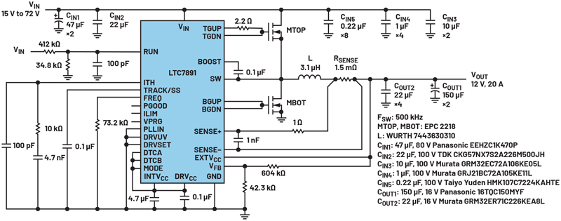
A simple way to avoid the critical evaluation process of protection functions in the power stage of the switch-mode power supply using GaN switches is to select a power supply controller IC. The LTC7891, single-phase, step-down (buck) controller is specifically designed for GaN power stage switches. Selecting a dedicated GaN controller makes a GaN power supply design simple and robust. All the challenges mentioned earlier are addressed and solved with such controllers. Figure 1 shows the simplicity of a step-down power design using GaN FETs controlled by a dedicated GaN controller.
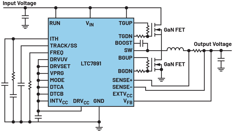
Figure 2. A dedicated GaN controller yields a robust and dense power supply circuit.
Click image to enlarge
Dedicated switching controllers offer the flexibility needed to work with different GaN switches available on the market today. Also, GaN switch technology is far from having finished its path of development, so future GaN switches will be different to today’s offerings. However, they might require slightly different handling. Devices such as the LTC7891 in Figure 2 offer a dedicated up and down gate drive pin for both switches. With this, the rising and falling slope of the gate voltage of the GaN switches can be controlled separately. This allows for driving the power stage with GaN switches with minimal ringing and overshoots.
In Figure 2, the most prominently visible difference to a heritage silicon MOSFET buck controller is the separate gate drive pins for rising and falling edges. However, many additional differences exist between the LTC7891 and controllers designed for silicon switches. There is an internal bootstrap switch to prevent the overcharging of the high-side driver during dead times. This is implemented reliably without the need for external components.
Another important feature is the smart near zero dead time control. This allows for reliable operation and yields significant power conversion efficiency improvements, while also allowing for high switching frequencies. The LTC7891 is rated for switching frequencies of up to 3 MHz.
One other unique feature is the possibility of accurately adjusting the gate drive voltage from 4 V to 5.5 V to optimize the VGS for different GaN FETs.
Using Any Controller IC
Engineers may also consider using a heritage controller IC and utilizing a driver stage optimized for GaN usage. This also allows for a simple and robust design. Figure 3 shows the power stage of a buck regulator implemented with the LT8418 driver IC. This driver comes in a very small WLCSP that enables very low parasitic resistances and inductances for low voltage offsets resulting from fast current changes.
Figure 3. A dedicated GaN driver controlling a power stage based on logic PWM signals from a heritage silicon MOSFET controller.
Click image to enlarge
One way to get first evaluation results is to use a detailed circuit simulation. LTspice offers complete circuit models that may be used for simulation free of charge. This is a convenient way to learn about using GaN switches. Figure 4 shows a simulation schematic with the LTC7891. A dual-channel version, the LTC7890, is also available.
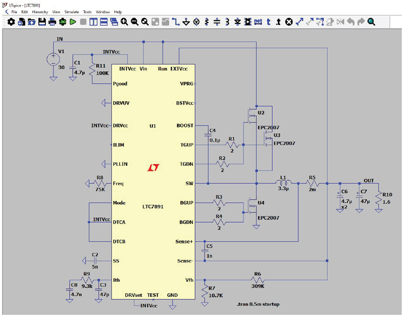
Figure 4. LTspice, a useful simulation tool for GaN power supplies.
Click image to enlarge
Integrating Wide Bandgap
While GaN technology is brilliant for building FETs and using them in an advanced power stage, GaN is not necessarily able, nor cost-effective enough, to be used as the control circuitry for a switch-mode power supply. Therefore, we will see a hybrid approach for the foreseeable future. The control will be silicon based with highly optimized control and drive circuitry to drive a high power GaN switch. This approach is technologically available today and it is cost competitive. However, it will require the use of multiple die in one circuit. Either with the GaN switches separate, or by integrating multiple die in one of ADI’s all integrated hybrid approach in a power converter IC or in a µModule power supply solution with the integration of many passive components including the inductor.
Growing large, high quality GaN remains a challenge. GaN on diamond is one way of processing GaN switches. However, since roughly 2010, the mainstream choice in GaN manufacturing is high electron mobility transistors (HEMTs) on silicon due to the larger possible wafer diameters and the lower associated cost with existing silicon processing infrastructure. Early technical challenges with this approach have been resolved. However the technology requires years of further development. In this case, GaN devices are made using GaN epitaxy on silicon wafers, so they are not grown as bulk crystals like silicon or SiC.