The advantages of using wide bandgap technology when designing an On-Board Charger (OBC)
Figure 1: Typical OBC electrical schematic
One of the most important technology revolutions today is vehicle electrification, and it is leading to a large disruption of the automotive industry. One of the sparks that ignited this new revolution was the CO2 emission reduction targets set by governments around the world, but it is not the only one. In truth, what is happening is an old story in science and technology. This is a time, when together with a growing awareness of the severe risk that humanity is facing, there are new technologies becoming mature and replacing old ones with better results and at more competitive prices. Those new technologies are power semiconductors, along with battery development and manufacturing. This is a trend that has become well established, and can no longer be stopped, and will drive the evolution of the automotive industry for the next few decades.
According to the YOLE intelligence report dated 2022, the global EV market is forecasted to reach nearly 50 million vehicle units by 2027, with a 2021-2027 CAGR of 21%.
Common silicon power devices for vehicle electrification are being to be replaced by WBG (wide bandgap) materials, such as SiC MOSFETs & GaN HEMTs (High Electron Mobility Transistor). The adoption of WBG materials improves the efficiency and the form factor of the systems. Despite their higher cost, WBG materials are in fact chosen more often due to their ability to provide extremely enhanced performance in all the key functional blocks of EVs. This article will highlight the advantages of using GaN HEMTs in On Board Charger (OBCs).
On Board Chargers
The time taken to charge the battery is a very important specification for EVs, both Plug-in Hybrid Electric Vehicles (PHEV) or Battery Electric Vehicles (BEV). The final customer decision on whether to choose between an ICE (Internal Combustion Engine) vehicle or an EV can often depend on the charging times. The faster the charging time, the higher the confidence that the customer will opt for a PHEV or BEV. Therefore it can be argued that the charging infrastructure plays a key role in EV market deployment. Charging can be both off-board (DC Fast Charging) and on-board (AC On-Board Charger).
The OBC is integrated in the vehicle, where there is an AC-DC conversion between the charging socket and the battery that receives the mains via a charging cable and connector. Typical AC power levels for OBC are: 3.6 kW for a single-phase, right up to 22 kW for a three-phase supply. DC Fast charging is supplied directly by an external DC charger with all power conditioning being done outside of the vehicle. The infrastructure is shared (commercial/public charging station) and the power rating is higher (≥ 50 kW).
OBC is the interface between the vehicle and the grid. It has to manage the electricity flow from the grid to battery. The OBC power level determines the charging time. The typical topology of an OBC is represented in figure 1, it consists of two main blocks; power factor correction (PFC) and the DC-DC converter. The PFC block is AC rectification with a high power factor that is almost always above 0.9, which delivers high level DC voltage. The DC-DC converter block has an isolated topology and it is soft-switching for higher efficiency and high-power density.
The power semiconductors normally used in OBC designs are 650V SJ MOSFET devices, but the introduction of WBG semiconductors in the form of gallium nitride has created real competition due to the wide bandgap material’s properties.
Click image to enlarge
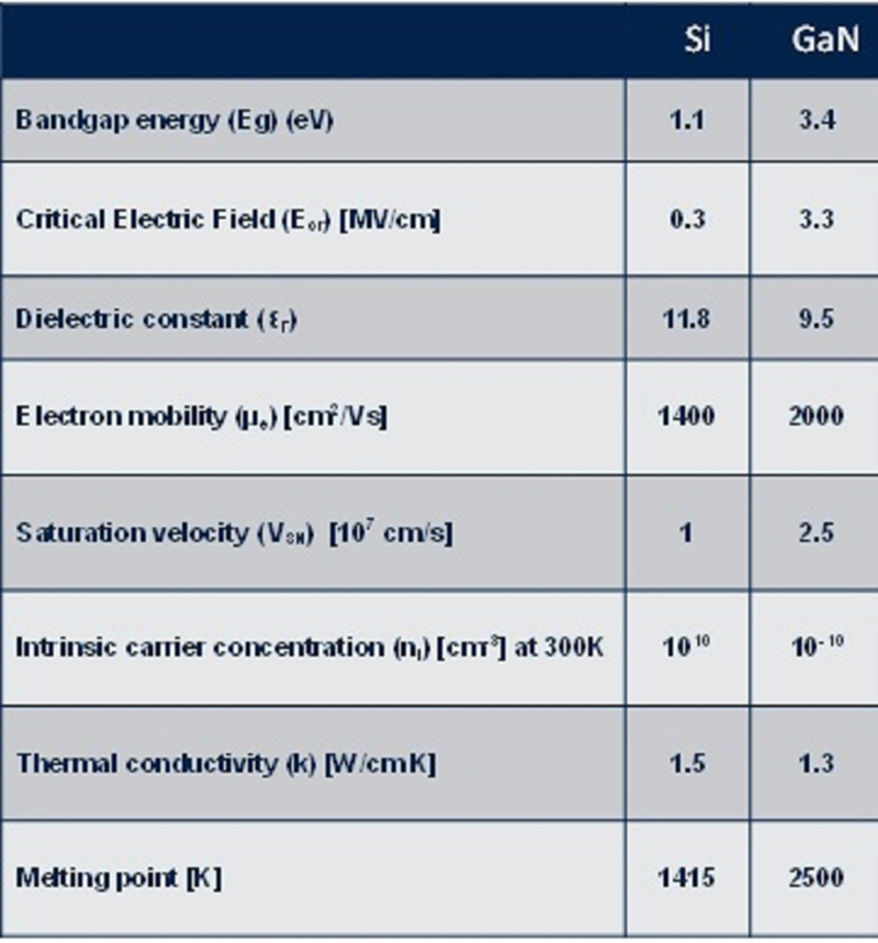
As shown in table 1, the bandgap energy and critical electric field are much higher in the GaN vs Si this allows very high breakdown voltage and lower Rdson and conduction losses. Moreover, much higher electron mobility and saturation velocity means higher switching frequency and lower switching losses.
PFC
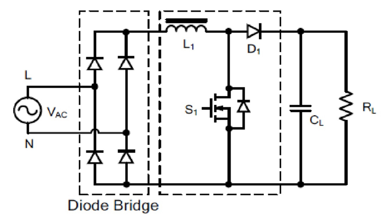
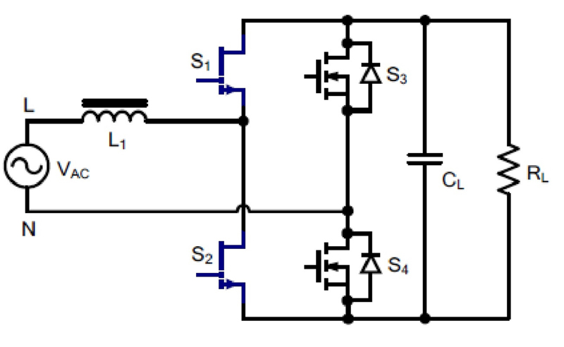
The PFC block in an OBC is based on boost topology. The traditional PFC circuit is based on a full-bridge diode rectifier topology, which has an efficiency of around <98% due to the diodes losses (see Figure 2). A more efficient topology that can be enabled using GaN HEMT technology is the bridgeless totem-pole PFC, which is able to reach an efficiency of 99% and is suitable for high-power OBCs. The bridgeless Totem Pole PFC circuit (see Figure 3) is derived from a traditional boost PFC, and replaces one half of the diode circuit with GaN transistors (high frequency branch) and the other one with two low Rdson High Voltage MOSFETs (low frequency branch). The advantages of the bridgeless totem pole PFC in respect to the traditional one can be explained by the following three points; improved efficiency, higher power density and bidirectionality. Bidirectionality enables a new trend in the industry, integrating EV batteries into the grid to cushion peaks in demand or production (V2G = Vehicle to Grid) and for VAR control (managing reactive energy on the grid).
Click image to enlarge
Click image to enlarge
GaN HEMT technology has smaller Qg and Coss, as well as a Qrr (reverse recovery charge) of almost zero, enabling lower switching losses. A comparison between an HV Silicon MOSFET and a GaN transistor with comparable Rdson and similar breakdown voltage (>650V) provides evidence on the different typical values of the main switching parameters (see table 2 below):
Click image to enlarge
DC-DC Converter
The DC-DC converter is the second power stage of the OBC. It converts the high-level DC input voltage to the voltage of the HV battery. Soft-switching conditions are needed to improve system efficiency and increase the power density. An LLC DC-DC converter is the most widely used topology, but it is not the only solution. The DC-DC conversion can also be achieved with ZVS PS FB, or DAB topologies. The optimal topology to choose for the OBC DC-DC converter design would depend on system characteristics, including the power density, if a very high battery voltage (800V) is to be used, if bidirectionality is required and the reliability needed. DAB topology is suitable for high power density systems or an 800V battery voltage (where a more elaborate multilevel approach is required when using 650V GaN HEMT devices).
An LLC DC-DC converter consists of three main blocks (see figure 1):
1. A square-wave generator. Q5 and Q6 transistors produce a unipolar square-wave voltage. Dead-time is inserted to prevent cross-conduction and establish ZVS (Zero Voltage Switching) operation.
2. A resonant tank, formed by the resonant capacitor and the resonant inductor connected to the magnetizing inductance of the transformer.
3. Rectification and filter. Synchronous MOSFETs (Q7 & Q8) together with the output capacitor smooth the secondary voltage to the output load.
Using GaN transistors in the DC-DC converter also allows reduced output capacitance (Coss), shorter dead-times, reduced third-quadrant losses and lower gate drive losses.The system can be optimized due to the fact that GaN HEMT enables a higher switching frequency. That higher switching frequency also means that the magnetic component sizes in the circuit can be reduced for a smaller final form factor. GaN HEMT technology, used both in the PFC stage and DC-DC converter, makes the OBC lighter and more compact providing a longer driving range
GaN HEMTs with breakdown voltages in the range 15V-300V and 600-700V are already well established on the market and commercially available from several suppliers, while very high voltage devices of 900V and over are still are in development or in R&D evaluation.
Conclusion
GaN HEMTs allow both a smaller power device (around 30% less) and tiny dimensions of the passive elements because of the higher frequency (up to 10 times higher), the total efficiency of the system is noticeably improved and the weight and space consumption of the total system is decreased: it makes an OBC lighter and better performing.
