Author:
Christopher Liu, Aanas Sayed, and Aniket Kulkarni, Nexperia
Date
02/20/2025
 PDF
PDF

Click image to enlarge
Figure 1. Six D2PAK MOSFETs with a total footprint area of 1,107 mm2
Today's automotive and industrial applications are faced with ever increasing performance demands. Power applications like inverters for electric vehicles (EV) and light electric vehicles (LEV), brushless DC motors, DC-DC converters, power switches and battery management systems can easily dissipate several kilowatts, which can result in individual discrete silicon MOSFETs operating beyond their capabilities. This often requires connecting several devices in a parallel configuration to handle the high current demands of these applications effectively. This approach helps prevent significant temperature increases and to maintain normal operating conditions. However, while generally effective, it does come with certain drawbacks.
This article explores these challenges and demonstrates how Nexperia's 100 V power MOSFETs, housed in the CCPAK1212 package, can reduce the number of MOSFETs needed in parallel to manage the high current demands of power-hungry applications, all while maintaining strong thermal performance.
Considerations When Connecting Power Switches in Parallel
The first disadvantage associated with connecting multiple MOSFETs in parallel is that it can result in unequal current sharing between devices. This is due to variations in the RDS(on) and other dynamic parameters between individual devices, meaning some end up carrying more current than others and hence experience higher heating levels. Over time, this can potentially cause performance and reliability issues. Another issue relates to unequal switching times resulting from the slight differences in the threshold voltage (VGSTH) of individual MOSFETs, potentially leading to reduced efficiency. These variations can be attributed to small but unavoidable tolerances that occur during the silicon fabrication process. Another significant disadvantage of this approach is the increased bill of materials and PCB space required for the application. For power electronics design engineers, minimizing the impact of each of these issues, without compromising the overall thermal performance of an application, is a key goal.
Comparing Parallel-Connected MOSFETs in Different Packages
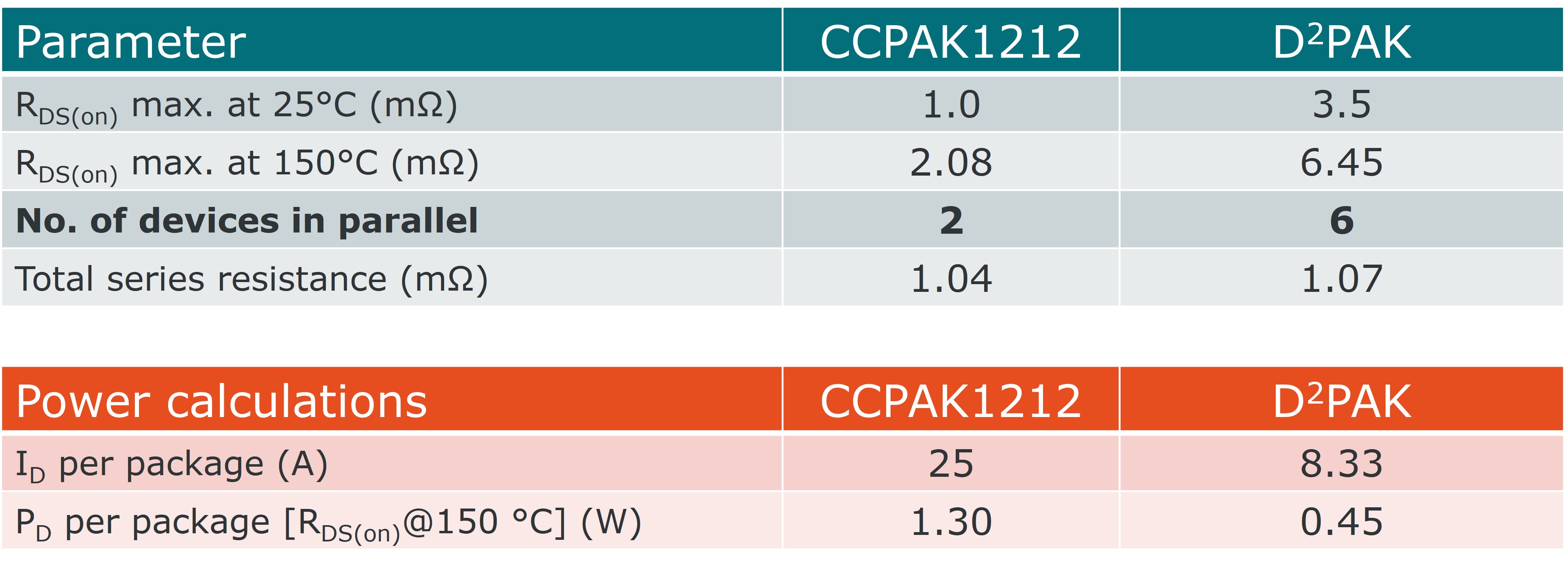
Nexperia performed thermal simulations on six parallel-connected 100 V 3.5 mΩ D2PAK-packaged MOSFETs (from an alternative manufacturer) operating as load switches in a typical high power 48 V application that was required to handle a continuous 50 A load current at an elevated ambient temperature of 120 °C (Figure 1).
The purpose of this investigation was to compare the thermal performance of this parallel arrangement of six switches to that of an identical application implemented using only two of Nexperia’s new 100 V CCPAK1212 MOSFETs connected in parallel, having a much lower total footprint area of only 351 mm2 (Figure 2).

Click image to enlarge
Figure 2. Two CCPAK1212 MOSFETs with a total footprint area of 351 mm2
To enable the calculation of realistic I2R conduction losses for each package type, the specified values of RDS(on) at 150 °C for each of the D2PAK and CCPAK1212 MOSFETs were used. At this temperature, the total resistance of two parallel CCPAKs is almost identical to that of six parallel MOSFETs in D2PAK packaging. Assuming equal current sharing between devices (for a total current of 50 A), each CCPAK1212 MOSFET conducts 25 A whilst each D2PAK conducts 8.33 A (Table 1). These figures were used as the basis for the thermal simulations performed on each device type.
Click image to enlarge
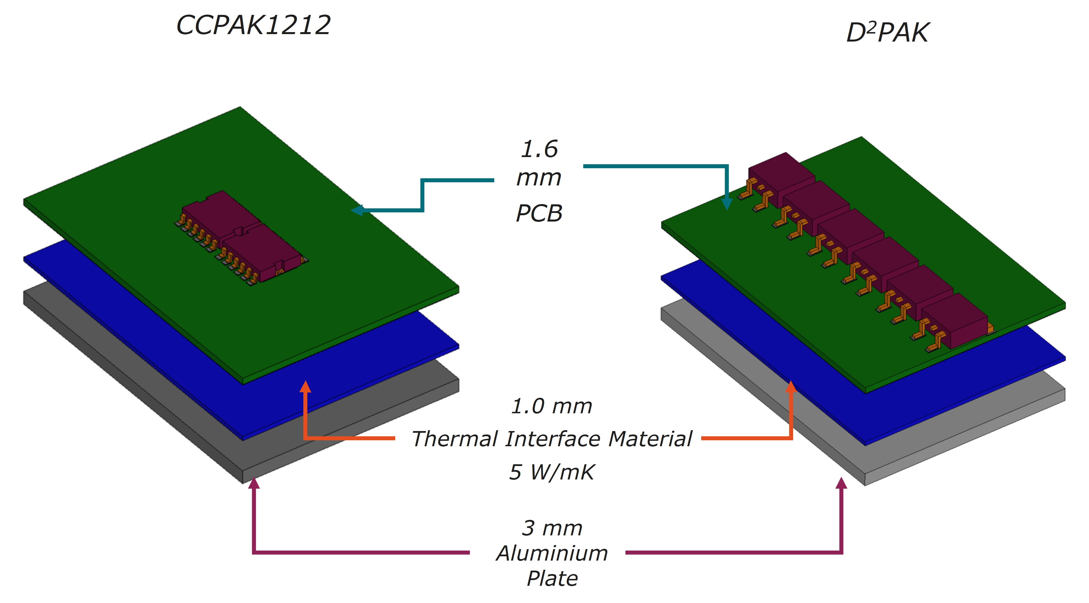
These simulations were based on a realistic PCB setup (Figure 3) using a 70 mm x 50 mm and 1.6 mm thick two-layer FR-4 PCB resting on a 3 mm thick aluminum plate with the same area. The PCB plate was separated with a 1 mm thick thermal interface material with a thermal conductivity of 5 W/mK.
Click image to enlarge
For stack up, the top copper plane used the recommended solder footprint with no additional traces and with 1 mm spacing between devices, while the bottom plane is a complete copper pore, as the ground is in both cases connected at the top and bottom with thermal vias for improved dissipation. Finally, drain and source nets were electrically isolated.
Results of Simulated Thermal Performance
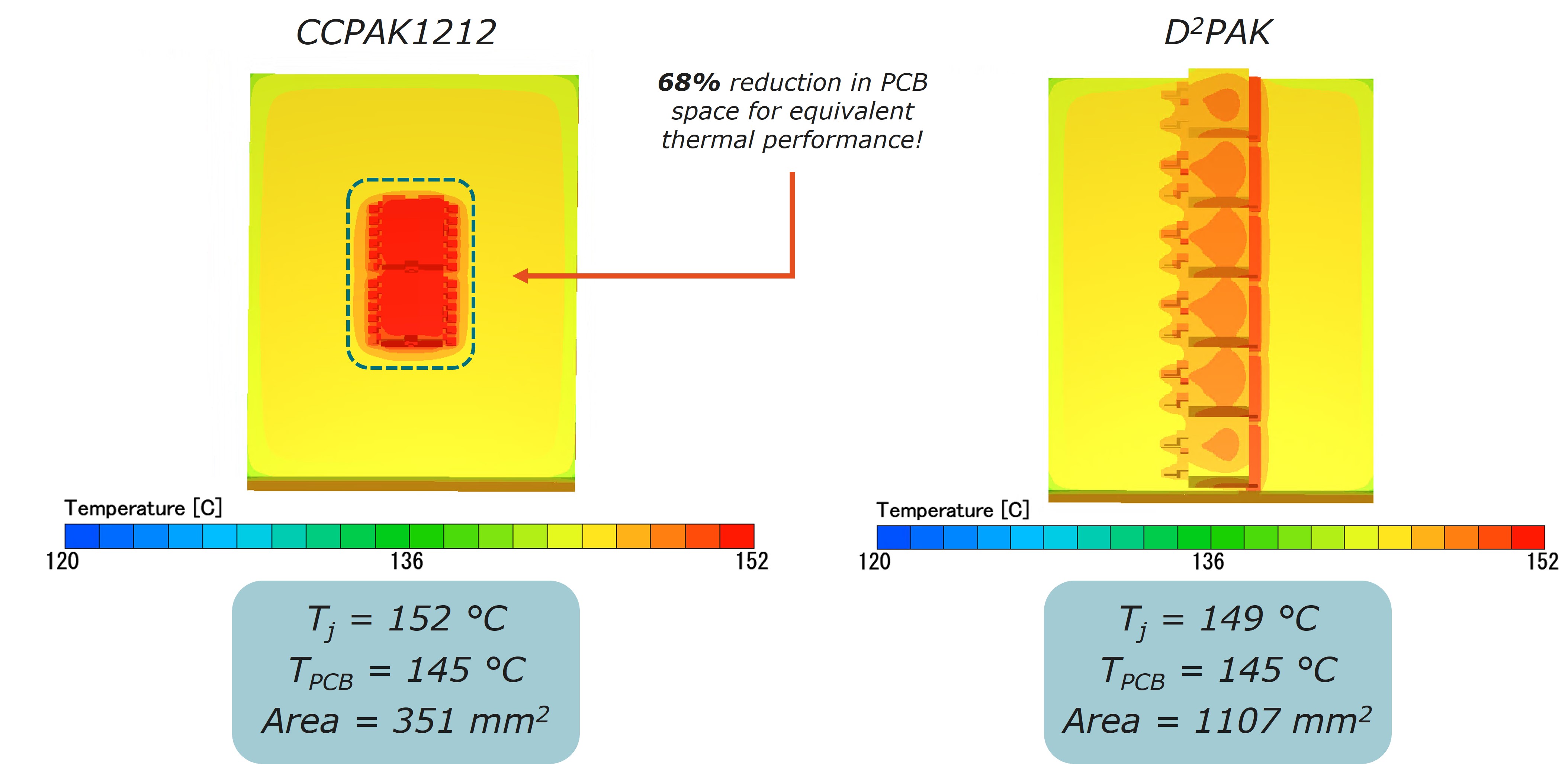
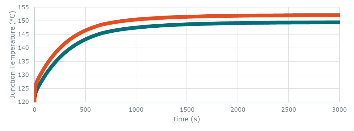
The results of the thermal simulations (Figure 4) showed that each of the CCPAK1212 switches delivered a comparable junction temperature and equivalent PCB temperature rises as the six D2PAKs in parallel while reducing the amount of board space by 68 %.
Click image to enlarge
Click image to enlarge
Applications advantages of CCPAK1212
The innovative copper clip design of CCPAK1212 allows MOSFETs housed in this package to deliver high current conduction combined with reduced parasitic inductance and excellent thermal performance. These features make them ideal for use in power-hungry applications like motor control, power supplies and renewable energy systems. The availability of top-side (TSC) and bottom-side cooling (BSC) options provides engineers with a choice of thermal extraction techniques, which can be helpful in applications where dissipating heat through the PCB is impractical due to the sensitivity of other components. Apart from 80 V and 100 V power MOSFETs, Nexperia offers application specific MOSFETs (ASFETs) in CCPAK1212. These devices, which target the hot-swap function in increasingly powerful artificial intelligence (AI) servers have an enhanced safe operating area (SOA) to provide superior thermal stability during linear mode transitions. All of Nexperia’s CCPAK1212 MOSFETs and ASFETs are JEDEC registered and are also supported by Nexperia’s interactive datasheets which enable designers to seamlessly integrate these devices into their designs.
Summary
Nexperia’s CCPAK1212 packaged MOSFETs are designed to address the thermal demands of next generation high power automotive and industrial applications. This article demonstrated how, compared to MOSFETs in D2PAK packaging, they can be used to reduce the number of MOSFETs connected in parallel without compromising the thermal performance of power electronics applications. Reducing the number of parallel connected devices offers several design advantages including mitigating the impacts of manufacturing tolerances on current sharing and switching times. Furthermore, using fewer devices also helps to simplify driving circuitry requirements while significantly reducing the required board space and the associated bill of materials.