High-efficiency, reliability and low power consumption makes new converters suitable for sensors used for assisted driving.
ROHM has recently launched the BD9S series of secondary synchronous Buck DC/DC converters qualified to AEC-Q100 for automotive applications. These offer high reliability and low power consumption in a compact form factor. This makes them very suitable for applications like radars, cameras and sensors which can be used for assisted driving.
The growing demand for safety requires a higher number of subsystems and at the same time, it is necessary to decrease the component size and quantities to reduce vehicle weight. Secondary converters must generate safe low voltage supplies from the output of a primary DC/DC (such as Rohm’s new BD9V100 device) with the highest possible efficiency and reliability. Figures 1 and 2 show a typical application and key features.
Click image to enlarge
Figure 2: Key Features of BD9S Series
Key Features
The key, user friendly, features offered by this lineup of devices can be summarized as :
· Multiple safety functions
· Fixed Frequency operation
· Compact and Space Saving
· Broad Line-up
· High efficiency
Multiple Safety Functions
The BD9S series devices include a range of safety functions to protect the device, especially against external faults, and to ensure safe and successful operation in any application.
If the input voltage falls too low for safe operation the BD9S series will stop switching and RESET itself using a Under Voltage Lockout (UVLO) circuit. It always re-starts with a soft start, where the time can be set be external capacitor, to suit different system applications.
If the feedback voltage (which is derived from output voltage by the resistor divider) falls below a threshold for long enough, the BD9S series will stop operation and then restart. This Short Circuit Protection (SCP) is intended to protect against temporary external shorts.
To minimize the output voltage overshoot when recovering from strong load transients or external fault conditions, the BD9S series includes an Over Voltage Protection (OVP) which monitors the feedback voltage and will turn OFF the output MOSFET.
To protect the high side MOSFET, and to avoid saturating the inductor (which would reduce the efficiency), the Over Current Protection (OCP) circuit limits the current every cycle.
For any power management device handling high currents over heating can be a risk. A Thermal Shutdown (TSD) circuit will disable the BD9S series if the junction temperature is too high. The BD9S series will restart automatically when the temperature falls.
When a fault (UVLO, SCP, OCP or TSD) occurs or the device is disabled, the BD9S series will stop supplying current. To ensure the output voltage discharges quickly, so that any connected device will RESET correctly, there is an integrated output voltage discharge switch.
Fixed (2.2MHz) Frequency Operation
The BD9S series switches at a fixed 2.2MHz frequency (tested and set during manufacturing), to reduce the size of the external components and prevent interference in the AM radio band.
Board Space (‘footprint’) Reduction
In many applications PCB space is extremely limited. The BD9S series switches at a high enough frequency to reduce the size of the external components and integrates the output power switches and compensation network to reduce the required ‘footprint’ to a compact 9mm x 5.5mm area (see figure 3) making it very competitive.
Click image to enlarge
Figure 3 : PCB footprint of BD9S11x with essential components
Rohm can also offer a 3mm square VQFN package with ‘wettable flanks’ (see figure 4), significantly improving visibility during solder mounting, which is a known quality issue with conventional QFN packages.
Click image to enlarge
Figure 4 : Structure of ‘Wettable Flank’ pins
Click image to enlarge
Figure 5 : Example Application Schematic of a BD9S11x
High Efficiency
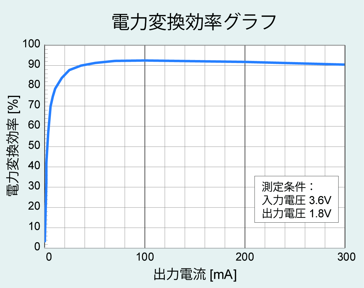
For DC/DC converters efficiency is critical both to reduce power consumption but also to avoid over heating of the device itself. The BD9S series achieves 90% efficiency (depending on operating conditions) see graph 1, using a current control loop to ensure rapid response to changes in the load.
Click image to enlarge
Graph 1 : Power Conversion Efficiency vs Output Current
The heat generated will depend upon input voltage, output voltage and load currents. For all DC/DC converters, the efficiency is reduced at lower load currents. The packages used in BD9S series include exposed heat sink to maximize heat dissipation. The practical thermal dissipation will depend upon many factors, such as the ambient air temperature and the PCB layout. A larger ground plane connected to the exposed heat sink will help to dissipate more thermal energy.
Broad Lineup
To fulfil a range of applications and provide flexibility, the BD9S series has been implemented as a range of devices covering different output voltages (either programmed during production or set by external resistive network) with maximum output current from 0.6 to 4A in two different ultra-compact packages: VQFN16FV3030 (3.0 x 3.0 x 1.0mm) and VSON008X2020 (2.0 x 2.0 x 0.6mm). These packages are leadless with wettable flanks. The suffix ‘xxx’ indicates the derivative.
Other Features
The BD9S series has an enable pin to reduce current consumption. After enable, the device always starts using a soft start where the duration is set by external capacitor.
There is a Power Good open drain output to indicate when the feedback voltage reaches the target. The open drain output allows connection to different power rails using a pullup resistor so it can act as a RESET signal for other devices.
Application
Rohm has designed the BD9S series devices to be easy to use in any automotive application, with a minimum BoM to reduce PCB area and save costs. See typical application diagram of the BD9S11x (figure 3). The correct method to select these components is carefully described in the datasheet, and an application note is under preparation.
ROHM Semiconductor, GmbH


