Author:
Ralf Otremba, Rafael Garcia, Daniel Makus, Ulrich Froehler, Lisa Holzmann, Infineon Technologies
Date
06/12/2024
 PDF
PDF
Click image to enlarge
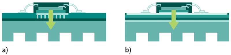
Figure 1: Bottom-side cooling (BSC) requires the use of thermal vias or an IPS board for heat dissipation
Maximizing power density is a key aim for designers of on-board chargers (OBC) in electric vehicles (EV) because lighter chargers reduce automobile weight which in turn helps to extend the range. Efficiency is one part of the equation for achieving this aim and in this regard, the advantages of silicon carbide (SiC) devices over silicon (Si) devices are well versed. Device packaging and cooling is the second, but less well-versed, part of the equation and has an increasingly important role to play in enabling more power-dense OBC designs.
To assist designers making the transition from through-hole to surface-mount technology, Infineon has developed double DPAK (DDPAK) and quadruple (QDPAK) SiC devices which employ top-side cooling (TSC) to deliver equivalent thermal performance as the through-hole counterparts but with the added advantage of having uniform package height. This article outlines the thermal advantages of these devices, before exploring potential new possibilities for the future of this innovative packaging technology. It presents a concept comparison between the thermal performance of on-package versus in-package direct copper bonded (DCB) devices and shows how chip-on-lead frame packaging enables the use of diffusion soldering for die attach, which has the advantages of being significantly thinner and offering superior thermal performance than conventional soldering.
Top-Side Cooling is Superior
While through-hole device (THD) packages like TO-247 and TO-220 are still widely used in many applications, they bring the disadvantages of having high manufacturing costs and the requirement to be manually inserted into the printed circuit board (PCB) before being soldered onto the underside of the board. For these reasons, THD is increasingly being replaced by surface-mount devices (SMD), the placement of which can be automated and results in higher throughput and better reliability.
SMD packages dissipate heat in either of two ways – bottom-side cooling (BSC) or top-side cooling. While both BSC and TSC packages can be assembled using automated pick-and-place machinery, TSC provides several advantages over BSC packages like D2PAK and DPAK, which conduct heat generated by the die downwards towards the bottom of the board-mounted device. This is because PCBs are not optimized for very high heat conduction and create a substantial thermal barrier for BSC devices, meaning additional thermal vias are required to allow excess heat to dissipate safely (Figure 1a).
A negative consequence of this approach is that it makes PCB trace routing more challenging because large areas of the board are given over to thermal dissipation elements. An insulated metal substrate (IMS) board (Figure 1) can improve the thermal performance of BSC devices but these are more expensive than traditional FR4 PCBs.
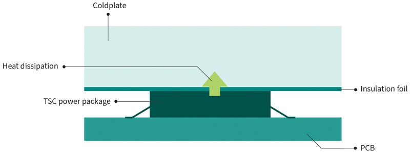
In TSC devices, the heat generated by the semiconductor die is extracted to the top side of the package which has an exposed pad onto which a cold plate (heatsink) is attached as shown in Figure 2.
Click image to enlarge
Figure 2: Semiconductor device employing top-side cooling (TSC)
Using this approach, thermal resistance is reduced by up to 35 percent and the thermal pathway is decoupled from the electrical connections on the PCB. This is significant because it makes PCB design simpler and more flexible, and brings the added benefits of smaller board area, higher power density and reduced electro-magnetic interference (EMI). Furthermore, because thermal performance is improved, board stacking is not necessary, so instead of combining both FR4 and IMS boards, a single FR4 is enough for all components and also requires fewer connectors.
These features reduce the overall bill of materials (BOM), which ultimately reduces overall system cost. In addition to improved thermal and power capabilities, TSC technology also offers optimized power loop design for increased reliability. This is possible because drivers can be placed very close to power switches. The low stray inductance of the driver switch reduces loop parasitic, which means less ringing on the gate, higher performance and lower risk of failure.
Infineon has developed double (DDPAK) and quadruple (QDPAK) SMD packaging for many of its power devices, including its range of CoolSiC G6 Schottky diodes, the new CoolSiC MOSFET families of 750 V and 1200 V devices paired with 650 V CoolMOS superjunction MOSFETs. These offer equivalent thermal capabilities but superior electrical performance to THD devices. Having a standard height of 2.3 mm for QDPAK and DDPAK SMD TSC packages with high voltage and low voltage options means complete applications like on-board chargers (OBC) and DC-DC converters can be designed using components which all have the same height. This reduces cooling costs compared to existing solutions based on a 3D cooling system.
Exploring Future Possibilities
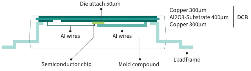
An additional feature of current TSC devices will be generated by using Al2O3-Substrate as direct copper bonding (DCB) for TSC-Isolation. This DCB could be inside the device package itself (DCB-in-package) as shown in Figure 3. One limitation of this approach is the necessary adaption of the chip-interconnect, die attach with a thickness of about 50μm is required. Furthermore, the thermal Device-Performance is limited by the thermal DCB-Performance.
Click image to enlarge
Figure 3: TSC-Isolation is currently implemented using in-package DCB
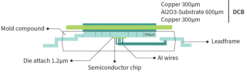
Infineon has proposed an innovative new DCB-on-package TSC implementation in which the semiconductor die remains directly connected to the lead frame, potentially offering several thermal advantages.
Firstly, connecting the die directly to the leadframe within the package offers additional heat-spreading capacity. Secondly, connecting the DCB on package would eliminate the adaption of the chip-interconnect & -redistribution. Finally, instead of using conventional soldering, diffusion soldering could be employed for die-attach, which would offer significant advantages, including allowing the thickness of the die-attach material to be substantially reduced from about 50 μm to only about 1.2 μm.
Click image to enlarge
Figure 4: TSC-isolation using DCB-on-package
Benefits of Diffusion Soldering for Die-Attach
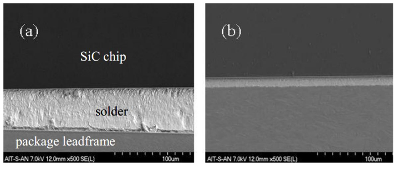
Due to the very high SiC-performance, SiC die are usually quite small (typically only a few mm²). Using conventional solder to attach such a small die to a package requires a well-controlled process because the surface energy of a solder drop can cause the die to tilt and this effect can subsequently hamper the wire bonding process.
This complication can be avoided by instead using diffusion soldering since the solder does not melt until it is brought into contact with the substrate. This method also allows multiple dies to be assembled on a single leadframe, as later heating steps do not affect the placement accuracy of the initial dies. This is because remelting of the solder does not occur, so there is no surface tension-driven displacement of the dies. In addition, this technique allows device size to be optimized as there is less solder squeeze-out which enables higher packing density. Reducing the amount of solder in a device significantly improves thermal conduction due to the superior material properties of diffusion solder and the reduced bond line thickness as shown in Figure 5.
Click image to enlarge
Figure 5: Cross section of die attach using (a) conventional solder and (b) diffusion solder. Diffusion soldering reduces bond line thickness. In (a), the solder is not uniform, causing the die to tilt
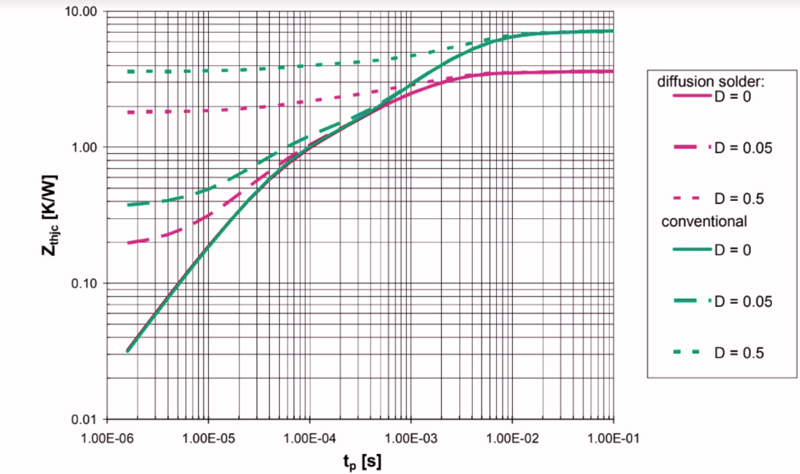
Measurements show that the thermal resistance between a Schottky diode junction and a package leadframe is approximately 40 percent lower compared to using conventional solder (Figure 6). This significant improvement in thermal performance means the maximum static current rating can be increased for a given chip area, allowing higher maximum power dissipation.
Click image to enlarge
Figure 6: Transient thermal resistance (ZthjC) vs. pulse length (tp) for different duty cycles. Data for conventional solder are shown in green, and data for diffusion solder in red
Thermal Simulation Results
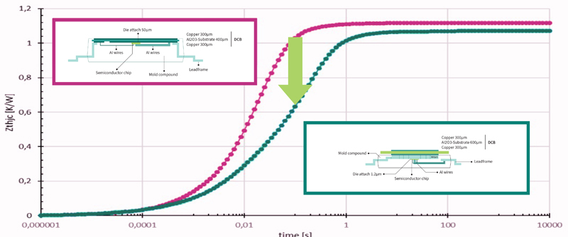
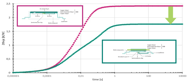
To evaluate the performance of its proposed new package structure, Infineon performed simulations on theoretical SiC dies measuring 4 mm2 and 14 mm2, comparing the thermal performance of the DCB-in-Package vs. DCB-on-Package approaches in response to an applied current pulse. The time-resolved simulation in Figures 7 and 8 shows that DCB-on-Package would offer better thermal performance than DCB-in-Package, allowing it to withstand higher magnitude currents (maximum and/or pulsed).
Click image to enlarge
Figure 7: Simulated thermal performance of DCB in-package vs. DCB on-package for a 14 mm2 SiC die
Click image to enlarge
Figure 8: Simulated thermal performance of DCB-in-package vs. DCB-on-package for a 4 mm² SiC die
Conclusion
Maximizing power density is a key aim for designers of on-board chargers in electric vehicles (EV) and component packaging and cooling mechanisms are increasingly important for achieving this. Infineon has responded to the needs of OBC designers by offering devices in uniform height, TSC DDPAK and QDPAK packaging, including its range of CoolSiC G6 Schottky diodes, CoolSiC MOSFETs 750 V and 1200 V and 650 V CoolMOS superjunction MOSFETs.