Thermal design considerations for thin power MOSFETs

Applications with high pulse currents benefit from thin, low RDS(on)MOSFETs but demand care in thermal design
Figure 1: SOA (a) and ZthJC (b) charts for the BSC014N04LS
Thermal challenges accompany almost all advances in power-electronic designs. Load cases not covered under a datasheet's parameters are often particularly problematic. Each new MOSFET generation generally marks a significant reduction in the area-specific on-state resistance—the product of RDS(on) and area. This means that a MOSFET with the same chip size offers dramatically reduced RDS(on) figures. Many optimization steps are required to achieve this outcome including altering the cell structures and scaling individual areas. The thickness of the silicon is usually also reduced, which can bring about shifts in thermal behavior. The reduction in silicon thickness lowers the thermal resistance, also reducing the amount of silicon available for temporary high loads. The challenge to the developer is to calculate these changes in the thermal behavior for each specific application and to optimize the design as appropriate. Datasheet values and the PSPICE library may not provide sufficient indicators for special cases, such as temporary loads, and analyses carried out using a thermal camera for such fast processes do not provide reliable values for the temperatures within the power device's package. Thin MOSFETs, such as Infineon's 40- and 60-V OptiMOS power MOSFET generation, feature on-state resistances to about half of the previous generation's values without changing chip sizes. This was only possible by reducing the thickness of the silicon. Chip thickness values in this voltage range are typically still in tenths of millimeters. Besides conventional switched-mode power supplies (such as synchronous rectifiers on the secondary side), typical applications in these voltage classes include motor controls in cordless power tools like screwdrivers and similar products. These designs must withstand high loads for short periods as they are often subject to such peaks under real operating conditions. It is therefore completely normal that a multiple of the rated current is permissible for a second, for example, when fully and securely driving a screw into a material. The resulting losses in the MOSFETs are briefly much higher than in rated operation. One possible design choice would be to reduce the losses by massive parallelization. However, this is not practical (or even possible in some cases) for cost and space reasons. On the other hand, such overload cases are one-time events from a thermal point of view since a repetition is not likely until many seconds later (for the next screw). Now, however, it is possible to buffer the power loss occurring during this short peak load and to dissipate it slowly over the lengthy period before the next power impulse. Silicon and the copper lead frame are ideal for this purpose. However, increasing levels of miniaturization have greatly reduced both structures in size already. In particular, high-performance packages, such as the SuperSO8, have fewer options for storing thermal energy due to their small volume. Manufacturers can use special IMS (insulated metal substrate) PCB designs for such SMD components. These consist, in principle, of an aluminum or copper substrate—usually between 0.5 mm and 3 mm thick—with a thin laminated insulation layer of enriched epoxy. The copper conductors and the SMD components are located on that layer. The metal substrate can operate as a thermal tank for storing thermal energy.


Thermal performance A useful starting point is an analysis of the datasheet areas that describe thermal behavior in relation to time and power dissipation. For example, the SOA and ZthJC charts (figure 1) depict the performance of a BSC014N04LS 40-V MOSFET that offers an RDS(on)<.sub> of 1.4-m? in a 5- x 6-mm SuperSO8 package. As the figure depicts, the MOSFET reaches a quasi-static state within 10 ms. An examination of thermal equivalent circuit diagram for the different silicon generations indicates that the chip volume plays a role only for short events below 100 μs. Even for very short load impulses, thermal energy can no longer be stored in the chip, but must instead dissipate first to the solder and lead frame and, after several milliseconds, to the environment. This means that chip volume does not play any measurable role in the case of impulses lasting at least one second. This is also clear when regarding the thermal properties of the materials—silicon, solder, and copper—in combination with their volume. This thermal behavior also reflects in the equivalent circuit diagram or PSPICE parameters. A thermal-equivalent circuit can depict the thermal system including the substrate (figure 2). In this example, the BSC014N04LS in its SuperSO8 package combines with the properties of an acceptably priced IMS. Here the specific thermal conductivity of the IMS's insulation layer is 1.3 W/(m x K) with a layer thickness of 76 μm. Calculating the system's temperature rise results in a value for theoretically homogeneous energy distribution, for which a ?T of about 51 K is generally acceptable. In a real system, however, the time constants play a major role. Purely mathematically,

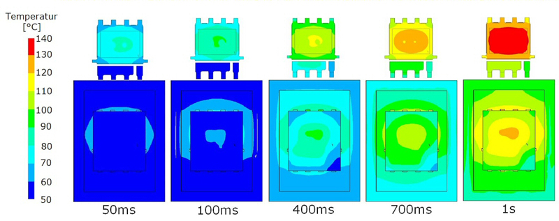
and non-homogeneous distribution of the temperature is to be expected. The real world behavior—the heating of the individual components in the system—is very much removed from the ideal model. The finite-element method offers a way of obtaining realistic values for each individual point of such a system, and of visualizing the values. Figure 3 shows how the temperature changes within one second for an assumed 25-W load. This corresponds to considerably more than 100-A drain current with 100% turn-on as a typical excess load that occurs when driving in a screw.

As a result of the MOSFET cells' good thermal connection to the copper lead frame, the maximum temperature difference between the chip and lead frame is only about 4 K (dark red and orange lines). Also clear is a short nonlinear interval—up to about 100 ms—after which all temperature behaviors are more or less linear. This is due to the previously mentioned short time constants within the component, as Figure 1 indicated earlier. Figure 4 also shows that these findings can easily transfer to another situation (power loss, turn-on relationship, starting temperature, impulse length, etc.) with sufficient precision. In the case of lower power losses or turn-on ratios, the line moves down in the according ratio. A shift upwards corresponds to greater power losses. Given the linear characteristics beyond about 100 ms, extending the lines displays longer impulse lengths. The 143-°C results for the example shown are close to the BSC014N04LS's permissible thermal limits—TJ(max) = 150 °C. The fact that the simulation assumes worst-case values offers additional security. It would be problematic, of course, if, for example, the impulse lengths were greater or if the power losses were more than 25 W because the reliability of the application could suffer under certain conditions without a change in the setup. An unacceptable reduction in the lifetime of the chip would be the consequence. Regarding the task in detail, there are a number of possibilities for improving the situation. Due to the non-homogeneous temperature distribution on the aluminum profile, it does not make much sense to increase it in size. The mounting volume may then no longer be acceptable and the costs would increase. It is much more advantageous to increase the thickness of the profile, which can greatly increase the effectiveness of the thermal tank for this brief impulse. However, this can result in cost and space disadvantages. Yet another design alternative would be to use an IMS material with superior thermal conductivity. The sharp rise in costs for this special material represents a drawback though. A further possibility is careful selection of power devices from the extensive range of available components. The developer can select an optimum combination, balancing cost and performance. In the setup shown above, a MOSFET with a low RDS(on), such as the 1-m? BSC010N04LS, proved to be a good choice with the added bonus of enhanced switching performance. Also available are 40-V chips with monolithic integrated Schottky-like diodes such as the BSC010N04LSI, which offer advantages, in particular, for fast switching. When assessing modern silicon technologies, consider whether the improvements in certain parameters, such as RDS(on) will result in disadvantages in other areas including thermal management. As the example given here shows, a reduction in the thickness of the silicon layer does not present a disadvantage in this or similar applications. Instead, the reduced thickness even lowers the thermal resistance between the MOSFET cells responsible for power loss and the copper lead frame, and the thermal capacity only suffers to an insignificant degree. The latter property only has an effect in the microsecond range in any case. Infineon Technologies


