Author:
Chip Brakeville, VP of Sales and Marketing, SemiQ
Date
07/25/2024
 PDF
PDF

Click image to enlarge
Figure 1: Example of threshold voltage as a function of temperature
Wide bandgap semiconductor technology has given electronics designers new degrees of freedom in their approach to high-power electronic circuitry. Silicon carbide (SiC) transistors in particular promise the ability to operate reliably and efficiently at higher temperatures than is possible with conventional silicon technology.
Conventional silicon has a bandgap energy of 1.12 eV. SiC, on the other hand, exhibits a significantly higher bandgap energy of 3.26 eV. This means that it requires roughly three times the energy to promote electrons from the valence band to the conduction band. The larger bandgap leads to a field robustness ten times that of silicon, providing higher breakdown voltages. Increased breakdown field can be leveraged to reduce device thickness, which leads to lower on-resistance and improved current-carrying capabilities. SiC also surpasses silicon in terms of thermal conductivity. The resulting three-fold improvement in heightened thermal conductivity translates to a lower temperature rise for a given power dissipation. This thermal performance not only enhances the overall performance and reliability of circuits based on SiC, it also allows for increased power densities.
Other benefits include a higher saturation electron drift velocity and lower intrinsic carrier concentration than found in silicon devices. The higher saturation drift velocity makes SiC more suitable for high-frequency applications. The lower intrinsic carrier concentration, thanks to the wider bandgap of SiC, allows these devices to operate at higher temperatures without excessive leakage.
The combination of factors that SiC provides makes it possible to do more than simply reduce the size of power converters and motor drives. The ability to operate in temperatures as high as 175°C means that it becomes possible to integrate power converters for cost and weight savings into motors, photovoltaic panels and other situations that generate large amounts of heat. However, to best exploit the novel properties of SiC, it is important to understand how environmental factors, such as temperature swings, affect SiC MOSFET behaviour. This is what SemiQ set out to do in an extensive series of tests of its 1.2kV SiC MOSFETs.
One of the important characteristics that require observation are the changes in threshold voltage due to temperature. SiC MOSFETs obey a negative relationship between temperature and threshold voltage that is broadly similar to that observed in silicon devices. But, as these devices can be operated at temperatures as high as 175°C, it is more important to understand the nature of the effect.
Research carried out in the early development of SiC showed that the temperature dependence of SiC transistors divides into two linear regions, with a higher slope at low junction temperatures, moving to a shallower slope as the device gets warmer.
To test this relationship on its devices, SemiQ used the method set out in the standard JEDEC JEP183 to achieve a more consistent measurement result. Under this method, the effective threshold voltage is regarded as the point where drain current reaches a set low current value based on die area with the gate and drain terminals shorted after the gate has been pre-charged. A typical result observed for the 1.2kV MOSFETs was a 0.79V reduction in threshold voltage at 175°C compared to room temperature. As a result, designers may want to consider applying a negative gate-source voltage when the device is switched off to prevent unwanted conduction.
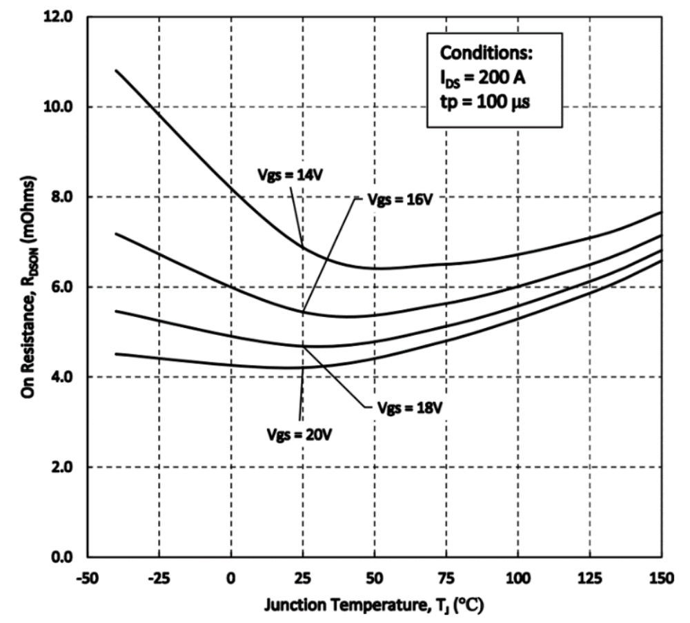
A second important test is of on-state resistance, which will contribute to many device behaviours such as self-heating and inefficiency if not controlled adequately. Temperature plays an important role in this characteristic, which is not confined to SiC devices. Below a certain threshold temperature, tests have shown SiC transistors exhibit a negative temperature coefficient. This shifts to a positive coefficient above that threshold. The gate-source voltage (VGS) plays a significant role in determining the circuit-level effects of this transition. A lower VGS emphasises the negative temperature coefficient and shifts the point at which the curve turns positive as shown in figure 2. This shows a lower on-resistance at high temperatures than is encountered under cold conditions.
The relationship between VGS and on-resistance can affect circuits where two devices are used in parallel to increase total power delivery. If the devices are expected to operate in cold or freezing conditions, there is a risk of one device become overloaded if its operating temperature is different to the other. Designers can avoid this situation by designing the circuit to increase VGS. Beyond 18V, the inflection point of the temperature coefficient occurs around 25°C rather than closer to 50°C for lower voltage levels. As the temperature reaches 100°C, the on-resistance finally surpasses that found at -40°C.
A higher VGS does not just result in a lower effective on-resistance but also increases drain-source current at higher drain-source voltages. As a result, a VGS should be at least 18V; however, 20V is recommended for this class of devices.
Click image to enlarge
Figure 2: Example of Temperature Dependency of RDS(ON) at Different VGS
As a key reason for employing SiC-based technology is to benefit from its high breakdown voltage, it is important to understand its characteristics. However, a sizable margin of safety is often built in. SemiQ has developed MOSFETs with an average breakdown voltage of more than 1500V, though they are rated in the datasheets as 1200V maximum devices to provide a wide margin of safety. Tests have shown this breakdown voltage increases slightly with temperature. The existence of the positive temperature coefficient makes SiC MOSFETs less prone to thermal runaway compared to some silicon devices. Thermal runaway is a phenomenon where temperature increases can lead to a rapid degradation of device performance, particularly at higher temperatures.
A related parameter that may need to be considered in designs is the rise in drain-source leakage current as the breakdown voltage is approached and how this current changes with temperature. This undesired current flows between drain and source when the device is turned off at the gate. Typically, this drain current increases with temperature, though the relationship between drain leakage current and breakdown voltages is complex. One benefit of SiC technology is that the breakdown voltage tends to increase with temperature. In tests of SemiQ’s devices, the voltage at which the slope of the leakage current significantly increases is typically only 50V across the entire operating temperature range of the device, as illustrated in Figure 3. Understanding these characteristics helps designers make informed decisions about thermal management in the target system and application margins, particularly if it will operate in low-temperature conditions.
Switching losses play a significant role in the overall performance of any MOSFET. In SiC devices, temperature-dependent effects control these losses. At elevated temperatures, the mobility of carriers can increase, increasing their speed in the channel. One consequence, shown in tests, is that the turn-on energy, Eon, can change with temperature while the turn-off energy remains almost flat.
The turn-on process involves charging the gate-source capacitance to reach the threshold voltage. The charging process introduces a delay, especially considering that the initial voltage across the gate-source capacitance is typically zero. This delay can cause higher turn-on energy losses.
Double-pulse tests (DPTs) can show how switching losses change with temperature, though care needs to be taken during these tests to reduce any parasitic components that inhibit switching performance. To do so, SemiQ engineers design package specific double pulse boards to minimize parasitic effects. Device under test temperatures are controlled with calibrated clip heaters or plate heaters.
The tests showed that the increased mobility at higher temperatures contributed to faster turn-on transitions. That results in reduced energy losses together with faster rise and fall times for the drain-source voltage (VDS) and current (IDS)waveforms.
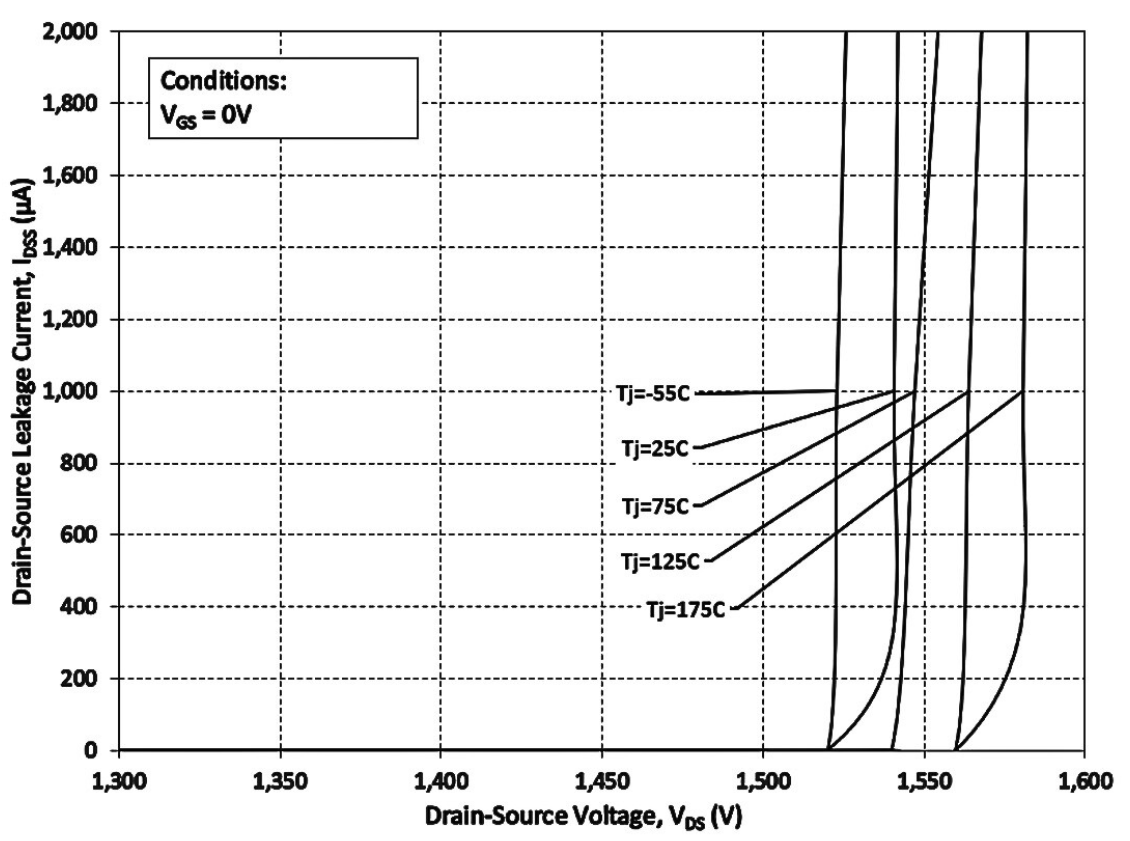
Click image to enlarge
Figure 3: 40 mΩ, 1200V SiC MOSFET Breakdown voltage versus Temperature
One other consideration for designers who wish to take advantage of SiC technology is the role of the body diode. The body diodes in SiC MOSFETs are generally understood to have much higher forward voltages compared to other diode types. As it is advisable to avoid using the body diode outside the dead time often employed in power conversion circuits, one strategy designers can adopt is to activate the MOSFET channel, where possible, when reverse conduction is required. This approach significantly reduces losses.
In summary, SiC MOSFETs have significant advantages in today’s high-power circuit designs, especially where high-temperature compatibility is important. Testing by SemiQ has confirmed these properties and the results provide valuable insights for engineers to leverage the strengths of SiC in circuits that need to guarantee breakdown voltages as high as 1.2kV under temperature extremes.