Individual chips are arranged horizontally with J-leadframes for surface mounting
PSD – What are the basic benefits of MLCCs?
JG - Multilayer ceramic capacitors (MLCCs) are compact, cost effective, and reliable. They have very low equivalent series resistance (ESR) values, which allows them to smooth high ripple currents. They are often used in place of and/or in parallel with electrolytic capacitors to improve system performance.
PSD – And why have MLCCs become so popular recently?
JG - Due to increasing miniaturization demands, there is a growing need for capacitors with high capacitance and improved temperature performance in ever-smaller dimensions. However, in the so-called HiCap range (≥ 1 µF) and in the mid/high-volt range (voltages from 200 V to over 450 V and 630 V up to 5 kV), they quickly reach their limits. This is because capacitors of size 1812 or larger are required here. Even with size 1210, which represents a certain performance optimum, multiple parallel connections and/or connections in series are required, which in turn requires a comparatively large board area.
There are usually other, taller components on the printed circuit board, so that in principle, more height is available for the capacitors, but this is not used in single chip applications. To save space, several capacitors can be combined into one component. They are stacked and connected in parallel. Compared to a single element, this gives them a lower ESR and equivalent series inductance (ESL) as well as a several times higher capacitance corresponding to the number of chips used. Two-chip elements are most commonly offered in sizes 1210, 1812, and 2220, although in extreme cases even they are available with up to ten chips and sizes up to approx. 30 mm × 50 mm. The individual chips are usually arranged horizontally with so-called J-leadframes for surface mounting. Through-hole versions are also available. However, they are used less frequently, partly because of the difficulty handling them in automated assembly, which leads to higher costs and longer production times. MLCCs structured with leadframes can also be used to increase the performance and robustness of single chips against thermal and mechanical loads.
Vertically stacked designs are also available for further optimization in terms of thermal stress and reduction of ESR and ESL ().
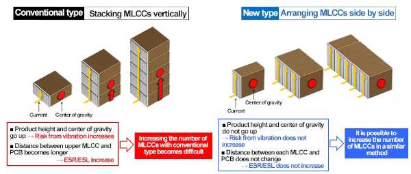
Figure 1 - Vertically stacked designs are optimized for thermal stress and of ESR and ESL reduction
PSD – Do the all work as basic capacitors, or are there different varieties of MLCCs?
Kemet offers parts without leadframes in its KONNEKT technology. The company uses an innovative TLPS (transient liquid phase sintering) material to create a leadframe and lead-free multi-chip element. This guarantees improvements in ESR and ESL as well as an increase in volume efficiency. These capacitors are available with horizontally and vertically stacked chips.
In addition, special ceramics with a positive DC bias are available from TDK. The company’s CeraLink devices are suitable for high frequency and high-temperature applications in power electronics, especially where space is limited and nominal currents, capacitance densities, and operating temperatures are high. The CeraLink capacitor consists of a PLZT (lead lanthanum zirconium titanate) ceramic in combination with copper inner electrodes. By balancing high current-carrying capacity and capacitance, CeraLink allows the number of capacitors required to be reduced compared to MLCC, taking into account overall cost. Unlike conventional ceramic capacitors, CeraLink capacitors have their maximum capacitance at the specified operating point (positive bias behavior), which increases proportionally to the ripple voltage ratio, making them the ideal capacitor for fast-switching wide-bandgap semiconductors such as SiC and GaN.


 PDF
PDF