Author:
Mike Zhu and Aparna Kumar, Qorvo
Date
09/20/2024
 PDF
PDF

Click image to enlarge
Figure 1: A modern approach to high efficiency AC/DC conversion
It is a credit to the community of designers and engineers working to increase efficiency, that according to the IEA, data center energy consumption only increased 20-70% between 2015 and 2022, while workload increased 340%. However, limits are approaching for power density in data centers with cabinets slated to dissipate 100 kW in the near future from around 30-40 kW today.
New standards have been introduced for efficiency and power density. Today, the highest Titanium rating is expected, requiring minimum 96% efficiency end-to-end for single-output 230 VAC-rated equipment at 50% load. High efficiency must also be maintained across the load range – minimum 90% at 10% load and 94% at full load.
Traditional AC/DC Topologies are Inefficient
Whatever the system architecture, there is AC/DC conversion and typically further stages of DC/DC conversion. Titanium levels practically excludes the traditional conversion approach of bridge rectifier, boost PFC stage and a full-bridge PWM stage using silicon MOSFETs switching at 100 kHz with diode output rectification and filtering. This scheme would result in an efficiency of around 85%, typically dropping off to a low level at light loads. To meet the Titanium level would mean reducing losses by a factor of more than 4x. Dropping switching frequency could reduce dynamic losses, but then transformer and filter magnetics size increase and power density becomes too low.
A solution is to use a ‘bridgeless’ PFC stage and a DC/DC conversion stage that utilizes zero voltage and/or zero current switching, followed by synchronous rectifiers (Figure 1). If wide bandgap semiconductors are used, there is an option to increase switching frequency substantially, to minimize magnetics size, although there are diminishing returns as core losses increase exponentially with frequency.
‘Bridgeless’ Totem Pole PFC Stage
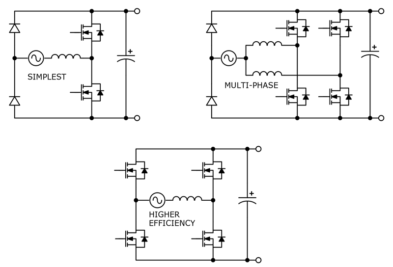
In its simplest form, the PFC boost diode is just changed to be a synchronous switch, the same as the main switch, then the two are driven to form boost switch and diode alternately, depending on the AC mains polarity, with diodes steering the return current back to the supply. For better efficiency the diodes can be replaced by synchronous switches toggling at line frequency or multi-phase approach can be taken to share out losses (Figure 2). For three-phase AC, it is relatively simpler still, with the ‘Vienna’ rectifier a popular implementation.
Click image to enlarge
Figure 2: Various implementations of a single-phase ‘bridgeless totem pole PFC’ stage
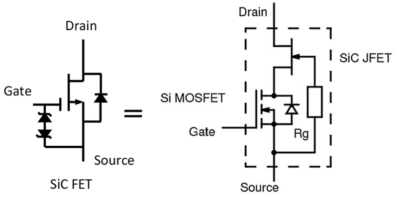
At high power however, the circuit is practically forced to operate in ‘hard-switched’ continuous conduction mode (CCM) where current levels are manageable but dynamic losses are high, from any current/voltage overlap and from reverse recovery of the switch body diodes, which conduct during switching dead-time. With silicon MOSFETs, target efficiency cannot be met without operating at a very low frequency and suffering large magnetics, but with silicon carbide switches, edge rates can be higher for low overlap and the body diode is much faster with lower reverse recovery loss. A better solution still is a cascode SiC FET (Figure 3), available from Qorvo, a cascode combination of a SiC JFET and a low voltage silicon MOSFET, which has lower relative on-resistance and a body diode that is equally fast but with a much lower forward voltage drop than a SiC MOSFET. Cascode SiC FETs are available from 650 V to 1700 V ratings and have the best figures of merit for on-resistance when compared with Si- or SiC MOSFETs or GaN HEMT cells. With its low dynamic and conduction losses, the cascode SiC FET can yield 99.28% efficiency for a bridgeless PFC stage, at 1.5 kW output from 240 VAC input, operating at 100 kHz, allowing a compact inductor size. This can be verified using the Qorvo FET-Jet on-line calculator using the 18 milliohm parts UJ4C075018K4S for the high-frequency switches. In the example, the two switches toggled at line frequency are uncritical as dynamic losses are low and at 1.5 kW, using UF3SC065007K4S cascode SiC FETs,the calculator puts their total losses at just 0.3 W each. The arrangement is capable of 3 kW output and at 10% load or 300 W, the circuit still achieves 97.53% efficiency, allowing for losses further down the conversion chain while still meeting the Titanium minimum efficiency.
Click image to enlarge
Figure 3: The cascode SiC FET – a ‘stacked’ silicon MOSFET and SiC JFET
DC/DC Conversion
The main isolation and DC/DC conversion stage in a data center power supply can be one of several high-efficiency topologies. The LLC converter is popular for its simplicity, its zero-voltage switching (ZVS) capability and potential to require just one magnetic component. Primary resonant current is relatively high though, so low RDS(on) switches are important to keep conduction losses low. Dynamic losses can be very low down to very light loads, but the circuit can lose ZVS under abnormal loading or start up, so precautions have to be taken to ensure stress levels are not dangerous under these conditions. The circuit switches with variable frequency to regulate the output and this can make EMI filtering less deterministic. Half-bridge and full-bridge versions of the LLC can be designed, no output inductor is required, and discrete or synchronous output rectification can be employed.
The CLLC converter operates similarly but with an additional resonant capacitor on the secondary side along with synchronous rectifiers, ensuring ZVS for all switches. Control can be by frequency modulation or phase shift. The symmetry of the topology makes it ideal for bi-directional power flow which is not a requirement in data center AC/DCs, so other topologies are typically chosen.
The Phase shift full bridge PSFB topology is a favorite for many as it operates at fixed frequency with simple 50% duty cycle antiphase gate drives to each leg in an H-bridge of switches. Regulation is achieved by varying the relative phase of the gate drives to the two legs in the bridge. A resonant inductor is required in the primary allowing ZVS, but an output inductor is required and maintaining ZVS to light load can be problematic.
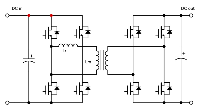
Another popular topology is the Dual Active Bridge DAB (Figure 4), which is similar to a PSFB circuit with synchronous output rectifiers but does not need an output choke. A primary inductor is required but this might be the transformer leakage inductance. The converter acts as a current source with power regulated which, as a consequence, regulates output voltage. In the simplest implementation of the DAB, all the H-bridge legs are driven at 50% duty cycle with some dead-time, and the legs are driven in antiphase to each other but the phase difference between primary and secondary gate drives is now controlled to regulate power flow. Control is complex and there are different modulation schemes with different control variables up to ‘triple phase shift’ where duty cycles of primary and secondary are varied as well as phase shift, with the advantage of potential reduction in RMS values of circulating currents. Output capacitor RMS current can be quite high and there is a concern about flux imbalance in the transformer, which can cause magnetic run-away, saturation and catastrophic failure. A DC blocking capacitor is a solution with a size and cost penalty, or other active control methods can be used to prevent the effect.
Click image to enlarge
Figure 4: The dual active bridge (DAB) topology
In the DAB, ZVS is naturally achieved in the primary and secondary switches at turn on, however, this relies on the output capacitance of the switches, COSS, being fully discharged during the dead time, implying that low COSS devices should be used and COSS variation with operating conditions carefully evaluated. With the simplest modulation schemes, turn-off occurs at the peak primary current, so this is a ‘hard’ transition and fast edge rates are needed to avoid excessive dissipation. Body diodes of the switches also conduct during dead time, so like the other topologies, their forward voltage drop and recovery energy should be low.
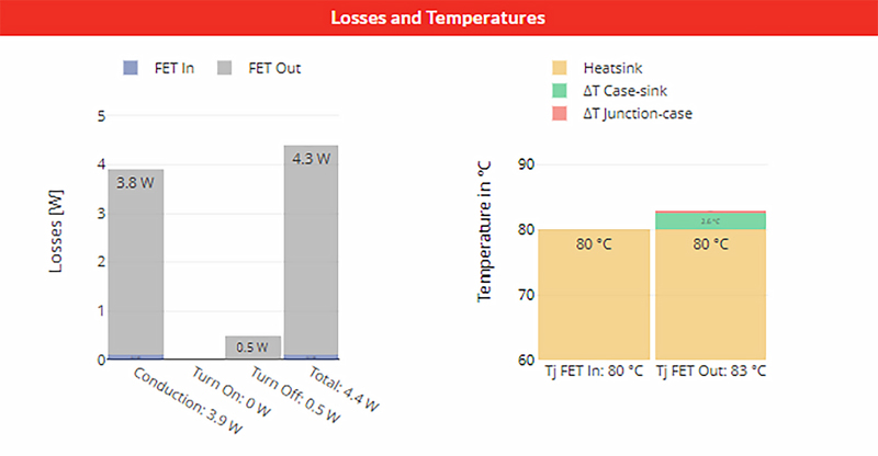
Cascode SiC FETs are again a natural choice for best performance in the DAB topology with their low dynamic and static losses compared to other semiconductor types. The Qorvo FET-Jet calculator can be used again to explore what performance is possible. With 1500 W output selected as 50% load for a DC/DC converter operating with 400 VDC input and 48 VDC output with 100 kHz operation and a 10 µH resonant inductor, the semiconductor efficiency achieved is 98.83%. At 3 kW, the efficiency is about 97.7% and at 300 W, efficiency is over 99%. Ohmic losses in the transformer and connections will add some losses but it is clear that along with a cascode SiC FET-based bridgeless PFC stage, the Titanium standard would be easily met. A screen shot from the calculator, Figure 5, shows that most losses actually come from the secondary side cascode SiC FET on-resistance. These were chosen as 6.7 milliohm UF3SC065007K4S types available from the standard Qorvo range. The 650 V device voltage rating is more than needed for a 48 V output so SiC MOSFETs or GaN HEMT cells might be chosen here with perhaps 100 V rating, and a consequential lower RDS(ON) and yet-lower conduction loss. Devices could also be paralleled for lower conduction loss.
Click image to enlarge
Figure 5: Screen shot of the Qorvo FET-Jet calculator results for cascode SiC FET losses in a DAB converter at 1.5 kW output


