In almost every case, the DC output from solar panels needs conversion to standard AC line voltages to operate existing loads or to feed into the grid
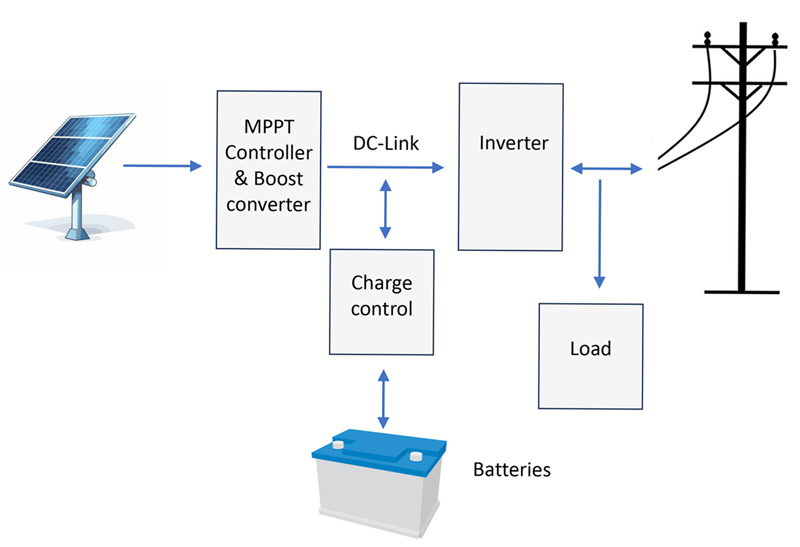
Figure 1: Solar power installation outline
PV installations vary in scale from an incidental power source in a domestic micro-grid generating a few hundred watts, to utility-scale, providing thousands of megawatts. In just about all cases, the DC from the solar panels needs conversion to standard AC line voltages to be compatible with existing loads or to feed into the grid. The panel DC is usually boosted to a DC-link using a maximum power point tracking (MPPT) controller; optional batteries on the DC-link provide continuity of supply and an inverter, often bi-directional, generates line AC (Figure 1).
With the wide range of power levels involved, solar arrays typically use ‘strings’ of panels with individual inverters with their outputs paralleled, rather than one high-power central inverter. Multiple smaller inverters might be higher total hardware cost, but they give the advantages of scalability and fault tolerance and can be deployed without heavy lifting gear. As a result, the largest part of the market is for inverters from a few kW to perhaps 200 kW, with DC-link voltages from 600-1500 V.
Semiconductor switches for the boost converter and inverter at the higher power levels have traditionally been IGBTs, with silicon MOSFETs viable for multi-kW ratings. However, in pursuit of higher efficiency and smaller installations, wide bandgap silicon carbide (SiC) switches can be considered. These are commonly available at up to a 1700 V rating with low on-resistance for minimal conduction loss and can be switched at high frequency with low dynamic losses. This enables smaller magnetics and consequent savings in overall system size, cost and weight.
SiC as a wide band gap technology not only provides high voltage blocking capability but also greatly reduces risk of failure from terrestrial neutron or cosmic rays, which is critical for reliability of solar systems.
On-resistance of a SiC MOSFET, RDS(ON), is still a limitation at high power however, as dissipation increases with the ‘square’ of current plus another multiplier due to temperature rise, unlike the nearly linear increase with IGBTs. But considering total device loss including switching losses, SiC is still much more efficient than Si. Moreover, SiC as a material provides 3 times better thermal conductivity to remove heat from the junction faster than Si.
SiC FETs Improve on SiC MOSFET Performance
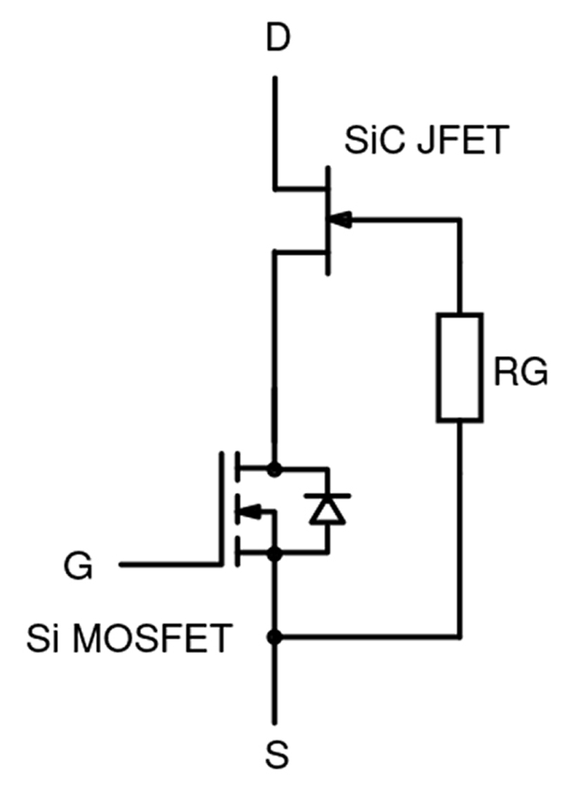
The SiC FET, pioneered by Qorvo, is an improvement on a SiC MOSFET in several ways. The SiC FET adopts SiC JFET technology with a cascode structure to reduce RDS(ON) further and employs advanced Ag sinter die attach to improve thermal performance to keep the switch junction temperature within bounds. This cascode combination of a SiC JFET and a silicon MOSFET (Figure 2) then has figures of merit (FOMs) for conduction and switching loss that set it ahead of competing technologies when comparing the same voltage class of device. At the same time, the SiC FET is normally off and has an easy, non-critical gate drive, typically 0-12 V with a stable threshold of about 5 V. In comparison, a SiC MOSFET needs a specific high-gate drive voltage for full enhancement, around 20 V, which is very close to its absolute maximum, and can have gate threshold stability issues. The SiC MOSFET integral body diode conducts in some applications, for example during switching dead time with inductive loads, and this causes charge recovery and forward conduction power loss. The SiC FET, however, is as fast as a SiC MOSFET but has a much lower body diode forward voltage drop, helping efficiency. Other parameters such as total gate charge, output capacitance and switching energy are also better than SiC MOSFETs.
Click image to enlarge
Figure 2: The SiC FET cascode arrangement
SiC FET E1B Modules
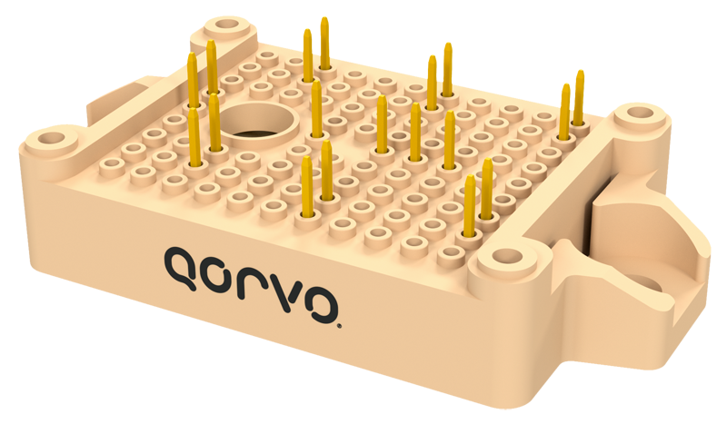
Until now, SiC FETs have been available in various discrete packages (TO-247, TO-220, TO-263, TOLL, etc.) and have found applications up to tens of kW. Qorvo has now launched a range of parts in the industry-standard E1B module format to address high power applications such as solar boost DC/DC and DC/AC inverter applications as well as for the EV charger and general-purpose industrial AC/DC markets (Figure 3).
Click image to enlarge
Figure 3: The E1B module package for SiC FETs
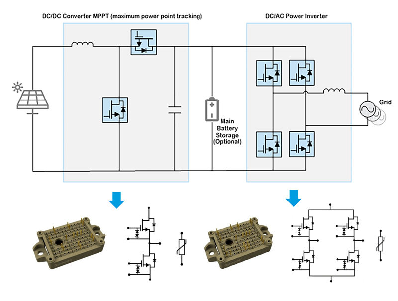
Rated at 1200 V, half-bridge modules integrate two SiC FETs and a thermal sensor and are available with RDS(ON) values of 19 milliohms and 9.4 milliohms, rated 69 A and 100 A maximum continuous current respectively at a case temperature of 25°C. Full bridge modules with four SiC FETs and a thermal sensor feature device RDS(ON) values of 70 milliohms and 35 milliohms, rated at 24 A and 36 A at a case temperature of 25°C. Tight integration of the die within the module enables close EMI control and high frequency operation without the limitation and variability of the interconnection of multiple discrete devices. This integration also greatly simplifies thermal mechanical design and assembly, while also helping to de-risk and shorten system development time. Figure 4 shows possible usage of E1B modules in a solar boost converter and inverter.
Click image to enlarge
Figure 4: SiC FET E1B modules in a solar power conversion application
Performance Metrics
Among wide bandgap and traditional silicon devices, SiC FETs have the best FOMs for on-resistance for a given die area RDS(ON).A and with output capacitance RDS(ON).COSS and related switching energy RDS(ON).EOSS. Importantly, these FOMs are still ahead of competing devices at 125°C as well as at 25°C. This means that in any soft or hard switched application, the SiC FET has a combination of low conduction and switching loss that is overall advantageous when comparing the same voltage class of device over a realistic operating temperature range.
Better still, the SiC FET E1B modules feature advanced thermal management through silver-sinter die attach which has a thermal conductivity of 130-250 W/mK compared with the traditional soldering technique at 23-53 W/mK. This results in a thermal resistance from junction to case of just 0.23 °C/W for the 1200V 100A half-bridge E1B module (UHB100SC12E1BC3N). For modules with stack-die-attach (Si low voltage MOSFET on top of SiC JFET), the power cycling capability is increased by more than 2X compared to SiC MOSFET-based modules, which is in line with Si performance. This is because when stacking, the high current carrying source wire bonds are attached to the less-rigid Si MOSFET, relieving the thermomechanical stress during power cycling tests. [Need a sentence here tying together the benefit of improved thermal management and 2x power cycling to provide longer product lifetime]
Optimizing Efficiency with SiC FETs
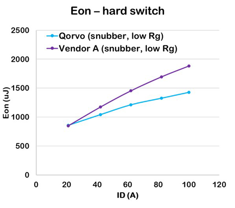
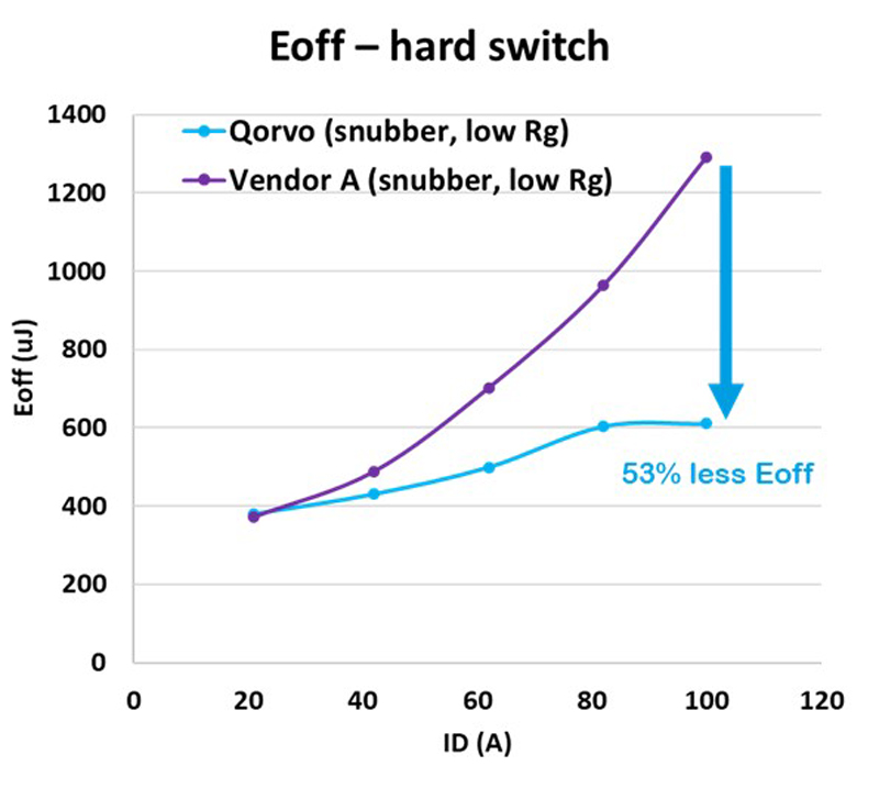
Power conversion topologies can operate in a soft-switched mode to minimize dynamic losses but boost converters typically do not do so at higher power levels. This is to maintain continuous (inductor) conduction mode, CCM, and keep current stress levels within manageable limits. Being hard switched, transitions have to be carefully controlled to minimize dynamic losses from voltage and current overlap, and this is typically done by selecting optimum gate series resistance with different values for turn on and turn off through a gating diode. With a SiC FET however, the gate of the SiC JFET is not accessible, and the series resistance is set in the die and is not adjustable. As an alternative, a small snubber can be used, typically with just surface-mount-size components, which Qorvo has demonstrated to actually be a lower loss solution, even with the dissipation in the snubber included. For example, measured values in Figure 5 (left) show around 32% drop in energy dissipated during a hard on-transition using a snubber and the Qorvo E1B module, compared with a competing part with edge rates controlled by a snubber and gate resistance. Figure 5 (middle) shows an even greater benefit of 53% less total energy in the off-transition of a hard-switched converter using the E1B module when using a snubber.
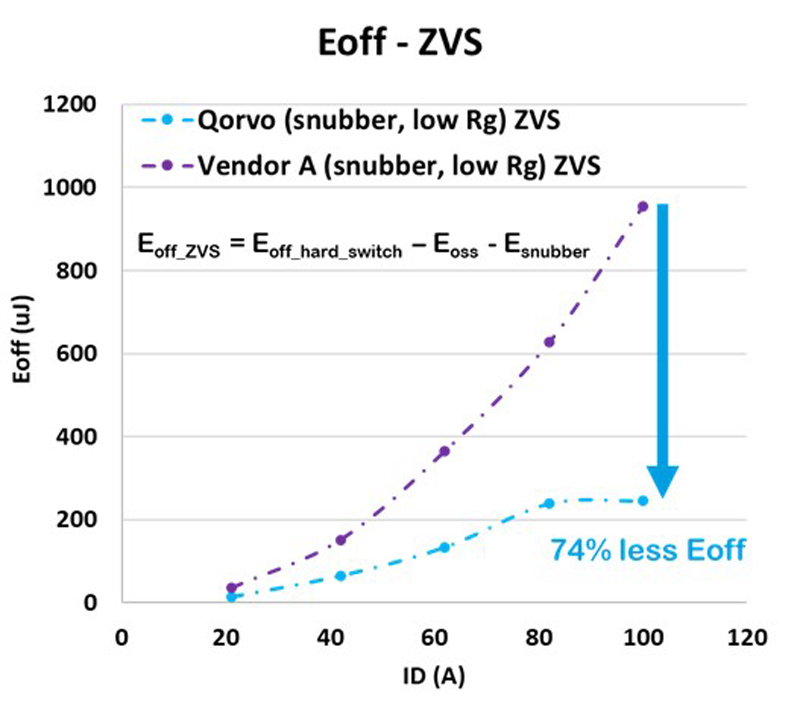
For a converter with soft switching of the turn-on transition (ZVS), turn-on loss is near zero. In such a case the snubber capacitance energy is recycled during ZVS and incurs no penalty for the turn-on loss that is seen in a hard-switched turn-on event. The graph on the right for energy dissipated on turn-off, with a soft-switched ZVS transition, shows that the Qorvo part with a snubber also has a strong benefit with 74% less energy dissipated than the competing part.
Click image to enlarge
Figures 5a, 5b & 5c: Qorvo SiC E1B module (UHB100SC12E1BC3N) switching loss benchmark with SiC MOSFET with recommended snubber
Dynamic losses can therefore be controlled to be lowest in class and, along with milliohm-level on-resistance and a high-energy avalanche and short circuit withstand rating, the SiC FET solution is a compelling proposition for high-efficiency solar converter/inverter designs.