Residential Solar: Part 2 of 4 Editorial Series sponsored by Infineon; Enhance string inverter designs with the latest SiC and SJ MOSFETs

Infineon’s new generations of CoolSiC™ and CoolMOS™ FETs are well placed for inverter designs in residential solar applications
Figure 1: Evolution of Infineon’s power transistors for string inverters
Recent advancements in power transistors have positively impacted the weight, size, and power density of solar string inverters. This coincides with the rising adoption of residential solar generation systems, which has touched 510 GW in 2023 alone, as mentioned in the first article of this four-part series [1]. The advancements include IGBTs, Si FETs, superjunction (SJ) MOSFETs, and most recently the wide-bandgap (WBG) semiconductors, contributing to increased power density and overall performance. This article, the second in the series, talks about the benefits to solar inverter design due to improvements in semiconductor technology.
The use of WBG-based MOSFET families like CoolSiC [2] and CoolGaN [3] has been increasing due to improvements in power density, cooling methods, and overall performance. Adopting WBG technologies reduces the stray inductance, lowers the BOM, increases the switching frequency, and improves the efficiency. This results in smaller housings and magnetic components, contributing to compactness and cost-effectiveness of power systems.
Improving efficiency in solar inverters
Traditionally, IGBTs have been widely used in three-phase or single-phase solar inverter designs. IGBTs, despite their low static losses, cannot support high switching frequency domains, leading to high dynamic losses. This limits their usage to only low frequencies (<40 kHz). In contrast, SJ MOSFETs can operate at higher frequencies (>100 kHz) and are feasible for low-power applications. However, IGBTs with their finite on-state resistance outperform these at higher power levels.
The performance of SJ MOSFETs deteriorates as power levels increase because the channel resistance increases with the square of the current through the MOSFET. They also suffer from a high reverse recovery charge (Qrr), slow body diode, and relatively high on-state resistance (RDS(on)), limiting their performance in inverters. These setbacks limit the conversion efficiency and power density of conventional single-phase solar inverters to ≤98 percent [4].
Two new approaches help achieve even higher conversion efficiencies:
a) Replacingconventional IGBTs and SJ MOSFETs with WBG SiC MOSFETs
b) Replacing traditional topologies with multilevel topologies to effectively utilize advanced SJ MOSFETs
Replacing IGBTs with WBG SiC MOSFETs
WBG semiconductor switches like SiC MOSFETs are gaining traction for their faster switching speeds and improved efficiency in solar applications. They offer benefits like lower on-state resistance, faster switching, lower capacitances, and superior thermal conductivity, making them a better choice over conventional SJ MOSFETs and IGBTs in PV systems.
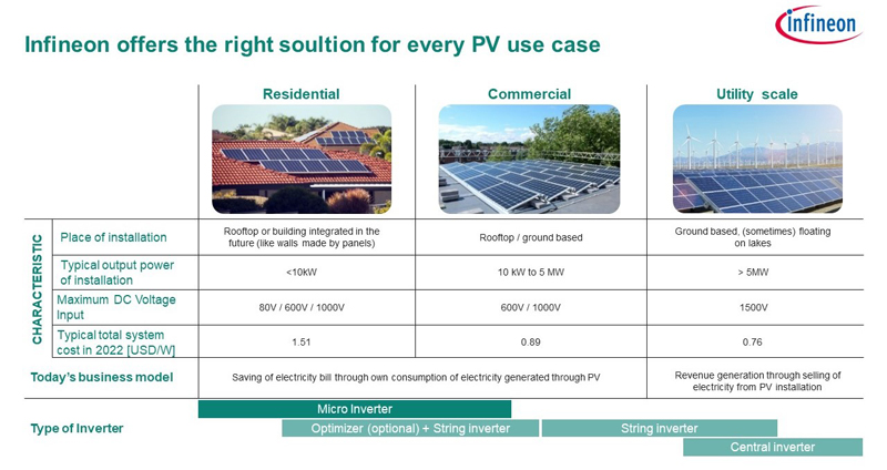
Infineon's recent portfolio, CoolSiC G2 MOSFETs (e.g., IMBG65R040M2H)[5], is based on the latest SiC trench technology. It offers an improved level of SiC performance compared to its predecessor, CoolSiC G1 MOSFETs (e.g., IMBG65R039M1H) [6] as shown in the figure of merit (FoM) comparison shown in Figure 2.
Click image to enlarge
Figure 2: Comparison of FoMs for CoolSiC G1 vs. G2 SiC MOSFETs
A lower output charge (Qoss) indicates a better switching energy efficiency, allowing the G2 device to operate with lower energy losses and enable faster switching speeds. G2 MOSFETs are evaluated by a new metric called the forward recovery charge (Qfr), which effectively captures the total switching charge. Qfr considers both the internal diode of the MOSFET and the charge in the output capacitance (Coss), providing a more comprehensive understanding of its switching behavior. From G1 to G2, the decrease in Qfr is ~45 percent, resulting in reduced switching losses and faster switching, leading to improved efficiency.
CoolSiC G2 MOSFETs have a reduced gate charge (Qg) that is 32 percent lower than G1 MOSFETs, also leading to faster switching speeds and lower switching losses. The lower gate charge in G2 MOSFETs makes them more sensitive to PCB parasitics, potentially causing VGS oscillation and voltage peaks. However, Infineon’s design has increased these limits for G2 MOSFETs, allowing the same external gate resistor values to be used for both generations and enabling the benefits of lower switching losses in G2 MOSFETs.
Click image to enlarge
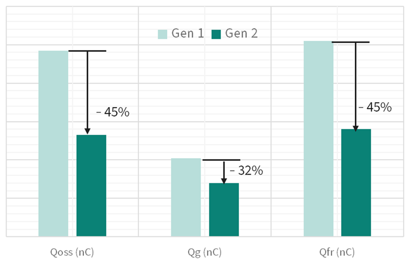
Figure 3: Normalized RDS(on) value vs. temperature comparison: CoolSiC G2 vs. G1 MOSFETs
CoolSiC G2 MOSFETs have a slightly higher RDS(on) rise with temperature than G1 MOSFETs, but this is offset by reduced switching losses, resulting in improved efficiency in target applications. The improved efficiency is due to channel improvements that shift the RDS(on) distribution to the devices’ drift region, thus enhancing process stability and reducing the typical-to-maximum RDS(on) margin [7].
CoolSiC G2 MOSFETs are designed for easy integration as a drop-in replacement for conventional MOSFETs, facilitating a seamless transition without major topology changes of the inverter.
Replacing traditional topologies with multilevel topologies
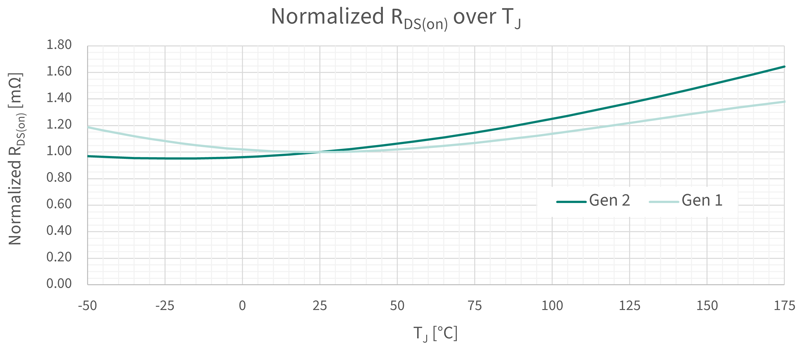
Traditional topologies based on IGBTs and SJ MOSFETs (H4, H5, H6, etc.) are widely used in single-phase solar inverters. However, a novel multilevel topology (Figure 4) based on high-voltage MOSFETs is sought after for its higher efficiency and power density.
Click image to enlarge
Figure 4: Replacing a traditional topology with a multilevel topology
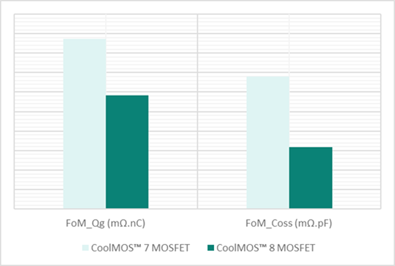
Infineon’s CoolMOS family has the best-in-class FoM, a measure of its performance, considering both conduction losses (ID² × RDS(on)) and switching losses (RDS(on) × COSS). The driving losses are calculated as RDS(on)× Qg. The lower the FoM, the better the MOSFET’s performance, indicating lower total losses. This is because a lower RDS(on) results in lower conduction losses, while a lower Qg and smaller COSS leads to lower switching losses. By minimizing the FoMs, the total losses in the MOSFET are minimized, leading to improved efficiency and performance.
Click image to enlarge
Figure 5: FoM comparison for CoolMOS 7 and 8
Infineon's CoolMOS 7 MOSFET (e.g., IPW60R040CFD7) [8]series is a high-performance MOSFET family that already offered high efficiency and power density. It features a lowRDS(on)and low capacitances (Figure 5), resulting in reduced power losses and improved switching performance. The latest CoolMOS 8 MOSFETs (e.g., IPW60R037CM8) [9] are designed for even lower power losses and improved thermal performance. The new product family has RDS(on)as low as 7 mΩ, making it suitable for high power-density designs [10].
Click image to enlarge
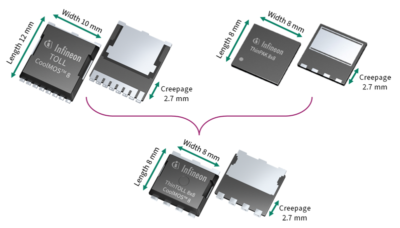
Figure 6: Merging TOLL and Thin‑PAK 8×8 to form Thin‑TOLL 8×8 package
The reduced heat dissipation of CoolMOS 8 MOSFETs simplifies thermal management and enables fanless or heatsink-free designs. CoolMOS 8 MOSFETs can reduce heat dissipation in single-phase inverter design by generating less heat due to reduced power losses. Available in SMD packages such as bottom-cooled Thin‑TOLL with a Thin‑PAK 8×8 footprint, these devices offer significantly better thermal cycling on board (TCoB) performance compared to other packages. By combining the features of TOLL and Thin‑PAK 8×8, Infineon’s Thin‑TOLL package can provide both high thermal performance and a compact, low-profile design (Figure 6). These packages can help reduce parasitic inductance, improve switching performance, and potentially lower assembly costs.
Conclusion
Infineon's latest CoolSiC G2 and CoolMOS 8 technologies, along with advanced SMD packages like Thin‑TOLL 8×8, provide superior performance in a compact form factor. This combination optimizes the performance in smaller packages specifically designed for solar inverter applications, helping with an even faster adoption of residential solar PV systems.
Don’t miss the next article in the series that describes using power optimizers to generate the maximum power from the available sunlight throughout the day.
References:
[1] International Energy Agency: Massive expansion of renewable power opens door to achieving global tripling goal set at COP28; https://www.iea.org/news/massive-expansion-of-renewable-power-opens-door-to-achieving-global-tripling-goal-set-at-cop28
[2] Infineon Technologies AG: Silicon Carbide CoolSiC™ MOSFETs; https://www.infineon.com/cms/en/product/power/mosfet/silicon-carbide/
[3] Infineon Technologies AG: GaN transistors (GaN HEMTs); https://www.infineon.com/cms/en/product/power/gan-hemt-gallium-nitride-transistor/
[4] Solar Inverter Design, Power Systems Design; https://www.powersystemsdesign.com/articles/solar-inverter-design/140/16354
[5] Infineon Technologies AG: 650 V CoolSiC™ G2 IMBG65R040M2HMOSFET in TO-263-7 package; https://www.infineon.com/cms/en/product/power/mosfet/silicon-carbide/discretes/imbg65r040m2h/
[6] Infineon Technologies AG: 650 V CoolSiC™ IMBG65R039M1H MOSFETs in compact SMD package; https://www.infineon.com/cms/en/product/power/mosfet/silicon-carbide/discretes/imbg65r039m1h/
[7] Infineon Technologies AG: 650 V CoolSiC™ G2 MOSFET; https://www.infineon.com/dgdl/Infineon-CoolSiC_MOSFET_650V_G2-ApplicationNotes-v01_00-EN.pdf?fileId=8ac78c8c8d2fe47b018dd18a40ef07fb
[8] Infineon Technologies AG: 600 V CoolMOS™ 7 IPW60R040CFD7 CFD7; https://www.infineon.com/cms/en/product/power/mosfet/n-channel/500v-950v/ipw60r040cfd7/
[9] Infineon Technologies AG: 600 V CoolMOS™ 8 IPW60R037CM8 MOSFET; https://www.infineon.com/cms/en/product/power/mosfet/n-channel/500v-950v/ipw60r037cm8/
[10] CoolMOS™ 8 600 V MOSFET, Infineon Technologies AG;https://www.infineon.com/dgdl/Infineon-CoolMOS_8_600_V_MOSFET-ApplicationNotes-v01_00-EN.pdf?fileId=8ac78c8c8eeb092c018f53db16de06e1&da=t