The increasing requirement in renewable energy systems and motor drive applications for ever-higher power levels is, as a consequence, driving the demand for power modules to provide higher levels of current. The conventional approach to fulfill this requirement is to look for dedicated high current power modules, but there is another way� This article describes the alternative approach of paralleling IGBTs and diodes within one power module to extend its power capability, for example using a 35A sixpack module as a 100A half bridge. The conclusion is that this approach provides an advantage due to the improved thermal behavior of several small chips rather than fewer big ones. The breakthrough in performance is seen when real life data of parameter variations within one power module are considered, instead of the datasheet values, which suggest a much higher spread than actually seen in real life. Figure 1 shows how a sixpack can be used as a half bridge.

The following calculations are based on the P700-F sixpack module from Vincotech, which uses Infineon IGBT3 Low Loss IGBTs and Emcon HE FREDs. Both components feature a positive temperature coefficient for their voltage drop at high junction temperatures. This is important in avoiding thermal runaway of individual components when paralleled. Switching behavior When paralleling IGBTs, special attention has to be given to the drive circuit. Because of the variation of the gate threshold voltage of the different chips, simply connecting the gates is not adequate. Instead, each gate has to be driven by its own gate resistor and therefore it own current source in order to ensure that the chip with the lowest threshold voltage does not clamp the voltage for the others and carry all the current. Furthermore, the layout of the emitter circuit has to be very symmetrical in order to minimize differences in emitter inductances and resistances. Even minor, unavoidable differences in the emitter inductances and resistances will generate compensation currents between the gate drive emitter connections. To limit these currents, the introduction of an emitter resistance in the drive circuit is strongly recommended. It is strongly recommended to use a resistor in the range of at least 0.5 Ohm, but not to exceed approximately 1/3 of the total gate resistance. To ensure real emitter drive sensing, the module needs to provide emitter sense connections with separate bond wires, as do the power modules from Vincotech. Moreover, any mismatch in the delay, rise and fall times of the driver circuit are to be avoided, as these will also result in a mismatch of switching currents and therefore switching losses of the different devices. Recommended is the use of a single gate drive circuit with individual gate and emitter resistors for the different IGBTs, as shown in Figure 2. If higher drive currents are required, a single driver circuit with individual push-pull driver stages is recommended.

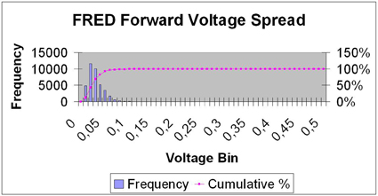
On-state behavior The on-state behavior is more critical. The datasheet for the P700 sixpack suggests a relatively large variation in IGBT collector-emitter and diode forward voltage. For the IGBT, the collector-emitter saturation voltage at 25°C is given as 1.7V typical and 2.25V maximum. No value is provided for the minimum voltage. Considering this information, the paralleling of chips cannot be recommended, since the current sharing among the individual IGBTs cannot be ensured. The situation is even worse for the diodes. In reality, however, the actual spread of the devices within one power module is much lower. This is due to the fact that they are picked from locations either exactly next or very close to each other on the same wafer, and will therefore feature extremely similar electrical characteristics. To determine the real voltage variation, Vincotech has collected data from more than 40 thousand modules produced in multiple lots distributed over a period of more than one year. This evaluation shows that the saturation voltage variation for 99.99% of the high side or low side IGBTs does not exceed 310 mV at 25°C and 450mV at 125°C respectively. For the FREDs, the value is 400 mV at 25°C and 490mV at 125°C. The distribution of the voltage spread within the measured series is shown in figure 3 for the IGBTs and figure 4 for the diodes. Table 1 shows the probabilities for different voltage spreads.


When considering current sharing, apart from the low or high side of the voltage variation of the IGBTs and FREDs, it is important to know what value the third device will exhibit. Again, instead of using a worst case view based on the datasheet voltage spread, the actual data collected from the 40 thousand modules can be used. Based on this information, the current sharing can be calculated for each module individually. The device with the lowest voltage drop is used to determine the voltage for the other two devices. By doing so, it is ensured that the best device will run with the maximum current level it is designed for and that the other devices will run at a lower current level well within their design limits. The current of the other devices can be calculated using the dynamic voltage slope of the saturation voltage for the IGBT or the voltage slope of the forward current for the diode. The total current of the module can be calculated as: Itotal = Inom (best device) + I2 + I3 And the current de-rating for the module can be calculated as: D = Itotal / 3 * Inom Figure 5 and 6 show the distribution of the de-rating for the paralleled IGBT and FRED section of the module. Table 2 shows the probabilities for the current de-rating.


For a design where the 13% de-rating for the IGBT and 25% de-rating for the diode is used, only 1 device out of 10.000 will exceed the targeted design limit of all devices running lower than the originally targeted current. Due to this fact, this single device out of 10.000 devices may exhibit lifetime, which is lower than expected. On the other side, the distribution curves show that, for the IGBTs, 90% of the modules will share the current within 2% and 99% within 6%. For the FREDs, the current sharing for 90% of the devices will be within 5% and for 99% within 9% respectively. With a design made using the 13% and 25% de-rating, the majority of the modules will run with a much better current sharing, thus running at a temperature lower than expected. This will not only compensate for the lower lifetime of the few devices, but also improve the overall lifetime and reliability of the design. Thermal behavior Using multiple smaller chips instead of one larger chip improves the thermal behavior, described by the thermal impedance of a device. This is due to the fact that not only the chip itself, but also a certain area around the chip, will participate in the transfer of heat from the chip to the heatsink. Figure 7 shows the improved thermal spreading when using two small chips instead of one large, with in equal total area in both cases.
This can also be seen when comparing the thermal resistance of the 100 A IGBT in the P569-F module with the 35A IGBT in the P700-F module. The thermal resistance junction to heatsink for the 100A device given in the data sheet is 0.57K/W. The resistance for the single 35A IGBT is 1.29K/W, resulting in an overall resistance of 0.43K/W, when 3 of them are used in parallel. This provides an improvement of about 25% in thermal performance, which compensates for some if not all of the derating required due to the non-ideal current sharing. Example using 35A Sixpack power module As an example, the performance of a 35A sixpack module used as a half bridge is compared to a 100A single chip half bridge module. The conditions and parameters used for the evaluation are shown below:
- Device: P700: Sixpack 35A / 1200V
- P569: half bridge 100A / 1200V
- Motor frequency: 50 Hz
- Cos phi: 0.8
- PWM frequency: 4 kHz
- Heatsink temperature: 80°C
- Tj max: 125°C


In the next step, the current de-rating is applied and the result is multiplied by 3 for the 3 paralleled devices. Table 3 shows the result for the IGBT and FRED for both solutions. The result reveals that the overall performance for the application at hand can be improved by 13% using the P700-F 35A sixpack instead of the P569-F 100A single chip half bridge. The actual improvement will vary for different application parameters and therefore needs to be evaluated at the most critical point. Conclusion The use of sixpacks as half bridges can boost the performance and enable the use of preferred modules and packages at higher power levels. Special care has to be taken regarding the drive circuit and current derating is to be considered when calculating the current of a single chip used in a multi-chip arrangement. Individual emitter sense down to chip level and symmetrical design are required of the power module, both of which are met by Vincotech modules. With the use of components in parallel, not only can higher current levels be reached, but also the reliability of the design is improved. www.vincotech.com


