Author:
Pete Losee, Senior Engineering Manager – Power Devices at Qorvo
Date
07/01/2023
 PDF
PDF

Click image to enlarge
Figure 1: Transient thermal impedance of Qorvo device UJ4SC07500L8S v. pulse width and duty cycle
The race to reduce power losses in semiconductor switches is being led by wide band-gap (WBG) devices and particularly SiC FETs, cascodes of a silicon carbide JFET and co-packaged silicon MOSFET. This arrangement produces a normally-off device with an easy gate drive and a trophy cabinet of ‘figures of merit’ that beat all competing technologies. A particular FoM is on-resistance per unit die area for a given voltage class of device RDS(A), which captures the combination of low static and dynamic power loss, and economy. Smaller die means more per wafer and lower device capacitances, with consequent lower switching loss. All good so far, but does a smaller die risk excessive temperature rise and reduced peak current capability? Quite the reverse, as we can show.
SiC FET On-Resistance is 4-10x Better than Competing Devices
Putting figures to the performance of a SiC FET, a 750V-rated device from Qorvo part UJ4SC075005L8S in a TOLL package, achieves an RDS(A) FoM 2.2x better than Gen 4 SiC MOSFETs, maintained across the temperature range. In practical terms, the device exhibits an on-resistance of 5.4 mΩ at 25°C and 9. 2mΩ at 125°C, 4 to 10 times less than silicon- or SiC-MOSFETs and GaN HEMT cells, which are only rated at 600/650V.
To leverage this ultra-low resistance, so that it translates to high current rating, SiC FETs from Qorvo in TOLL packages use silver sinter die attach and advanced wafer-thinning techniques, resulting in just 0.1°C/W thermal resistance from junction to case. As a bonus, the maximum junction temperature for the SiC device is 175°C, compared with silicon at typically 150°C. As a consequence, a single device could pass 80A continuously, fixed to a modest 0.58°C/W heatsink, with the junction at 175°C and in an ambient of 85°C. This is from a TOLL package just 9.8mm x 11.65mm footprint, 2.3mm high.
SiC FET Peak Current Rating is Far Higher than Continuous
The TJ(Max) figure for a SiC device and its current rating is effectively set by the packaging used – silicon carbide as a material is actually capable of working safely to in excess of 500°C. Even if we limit the transient maximum to 175°C in the JFET of a cascode SiC FET, there is clearly the potential to handle peak currents of many multiples of the continuous rating when starting from lower temperatures. The time limit for a given peak current is set by the thermal capacity of the die and its immediate connection to the internal copper leadframe and can be characterized by a transient thermal impedance plot for a particular die and package. Figure 1 gives the values for a Qorvo UJ4SC075005L8S device.
As an example, from the plot, a single 100µs pulse will cause a transient increase in junction temperature of about 0.015°C per watt of power dissipated, whereas if the same pulse repeats with a 50% duty cycle, the increase is to about 0.07°C/W continuously. At about 10ms pulse duration, the thermal impedance tends toward the steady state value and at more than one second duration, pulses with less than 50% duty cycle can be treated as individual events, as the junction cools off completely between pulses.
What this means in practice for the example device UJ4SC075005L8S is shown in Figure 2. In this instance, the device case is soldered to a copper plane on a PCB with copper thermal vias through to a back-side aluminum heatsink held at 50°C, separated by an insulating thermal interface material (TIM), adding some thermal resistance. In this arrangement, the continuous rating is 89A, but up to 588A peak current can be handled for a 500µs single pulse before the junction reaches 175°C. The Figure shows the intermediate values of pulse current and allowable durations. The junction cooling down with multiple thermal time constants after the current pulse can be seen, as well as the overall worst-case heating and cooling time of about one second, after which the pulses can be considered as single events.
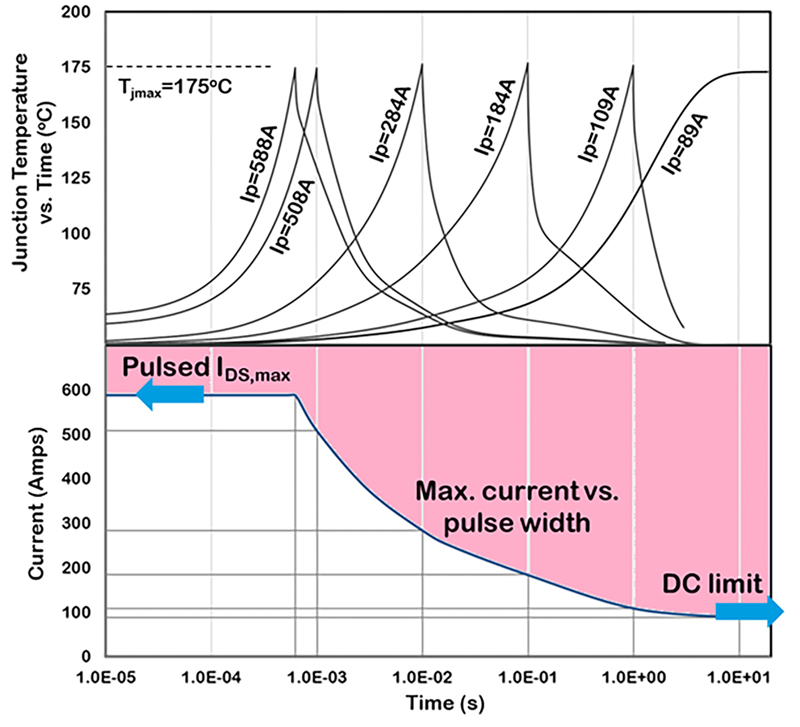
Click image to enlarge
Figure 2: Actual peak current capability of part UJ4SC075005L8S for a maximum junction temperature of 175°C v. time and pulse width
Under other conditions with less interface thermal resistance to a large heatsink, the maximum continuous current for the device can be up to 120A, limited by the internal bond wires.
Comparing SiC FETs and Si-MOSFETs
The results look good, but how do they compare with silicon MOSFETs, currently used in lower power solid-state circuit breakers for example? A familiar measure often seen for fuses and other devices that handle surge current is the ‘I2t’ rating and, in the TOLL package, the SiC FET is around 8x better than a Si-MOSFET. Figure 3 shows the comparison in the same physical arrangement as Figure 2 with our example SiC FET withstanding 588A for 500µs compared with the Si-MOSFET rating of only about 200A, an ‘I2t’ difference of 8.6x.
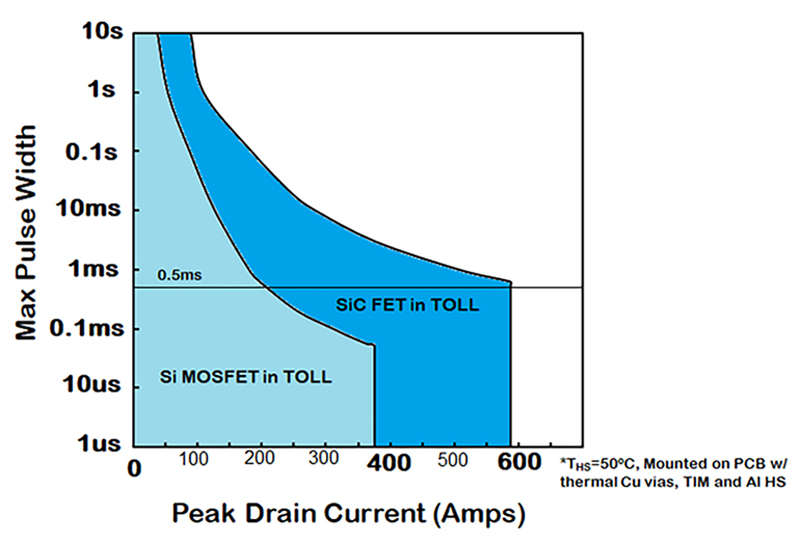
Click image to enlarge
Figure 3: ‘I2t’ rating compared between a SiC FET and Si-MOSFET
Further Advantage of High Peak Current Rating
Clearly the superior pulse current rating of SiC FETs gives a better safety margin under overload conditions in any application, but there are further advantages: SiC FETs are particularly suitable for power conversion circuits with inductive loads where voltage overshoot is inevitable. The devices have a robust avalanche capability, 316 mJ/single pulse in the case of the UJ4SC075005L8S. Also, board mounted DC/DC converters in servers and similar applications are increasingly required to have a high peak power rating in a small form factor, driven by data-intensive applications such as AI, machine learning and streaming.
The converters are now often designed with the assumption that junction temperatures will be driven toward their maximums and potentially higher, at some duty cycles, by peak currents experienced. Junction temperature information is fed back by sensors and prediction algorithms using digital control, typically via PMBus, to provide instructions to the load to ‘throttle back’ as necessary to avoid the switch junctions exceeding their absolute maximum. Again, the high margin provided by SiC FETs provides confidence in reliability and lifetime of the power system.
In these and similar applications, the high peak current rating of the SiC FETs can potentially reduce the need for multiple paralleled devices, with the corresponding savings in device cost and board area.
Solid State Circuit Breakers Benefit from High Peak Current Withstand
Solid state circuit breakers are used specifically to react to high fault currents, and SiC FETs and JFETs are increasingly used for their low voltage drop, displacing IGBTs, particularly at lower current levels. Fault currents can still be very high though and the peak current rating of SiC FETs is a benefit here, adding robustness and allowing the over-current detection circuitry to incorporate a longer delay before reacting, making it more immune to ‘nuisance’ triggering.
Conclusion
Small-form factor SiC FETs with peak current ratings in the hundreds of amps are ideal components in modern power conversion applications where high power density and peak load handling are required. Metrics show that the parts are significantly better than competing GaN and Si- or SiC-MOSFET parts in the same voltage class. The device described can be seen on the Qorvo website, along with a wide range of alternative parts suitable for a variety of applications.


