Author:
Ally Winning, European Editor, PSD
Date
07/03/2024
 PDF
PDF

An exhibitor demonstrates products at PCIM 2024
According to the organizers, this year PCIM had 637 exhibitors, a record number, with 60% coming from outside Germany. In total, over 18,000 visitors attended the exhibition.
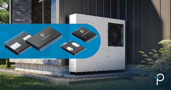
Nexperia

As expected, the most popular vertical market at the exhibition was the automotive one. There were lots of announcements on that subject, especially concerning SiC technology. Nexperia claims that the company’s SiC technology is a great jack of all trades. It provides good stats across the board instead of concentrating one one or two individual specifications.
The company announced at PCIM that its PSC1065H-Q 650 V, 10 A SiC Schottky diode is now approved for automotive use. Additionally the device is now available in real-two-pin (R2P) DPAK (TO-252-2) packaging. Nexperia also used the exhibition to launch an extended portfolio of industrial-grade devices with current ratings of 6 A, 16 A, and 20 A in TO-220-2, TO-247-2, and D2PAK-2 packaging.
The merged PiN Schottky (MPS) structure of the devices is intended to provide additional robustness against surge currents, eliminating the need for additional protection circuitry. This reduces system complexity and provides solutions with smaller form factors. In addition, Nexperia’s ‘thin SiC’ technology delivers a substrate that is one-third as thin as originally, reducing the thermal resistance from the junction to the back-side metal. This results in lower operating temperature, higher reliability and device lifetime, higher surge current capability, and lower forward voltage drop.
Power Integrations
Another area at PCIM that was very popular was electric motor drivers. It is a huge market, where there is currently lots of innovation using wide-bandgap materials to meet new efficiency regulations. Power Integrations originally developed its BridgeSwitch family for motor applications. Now, the company has launched its second generation of devices, with increased power handling and added features to make the range even more attractive to designers of motor systems.
The BridgeSwitch-2 motor-driver family of high-voltage integrated half-bridge (IHB) ICs can now be used in designs of up to 746 W. The ICs integrate high- and low-side drivers and advanced FREDFETs with integrated lossless current sensing, which together can bring inverter efficiency of up to 99%.
The BridgeSwitch-2 ICs can also handle operational exceptions in hardware, which permits the use of IEC 60730 Class A safety software, reducing certification time. Quiescent BLDC inverters can now be put into sleep-mode, reducing driver power consumption to under 10 mW and thereby leaving more power for other duties such as monitoring.
The IHB architecture halves the component count and cuts PCB space by 30%, compared to discrete designs by eliminating shunt resistors and signal conditioning circuitry. BridgeSwitch-2 motor drives use built-in, hardware-based low- and high-side over-current protection to meet IEC 60335-1 Class A requirements.
https://www.power.com/products/bridgeswitch/bridgeswitch-2?utm_campaign=BridgeSwitch-2
Microchip
One of the main trends I noticed at PCIM was that manufacturers were increasingly focussed on making their wide-bandgap products more accessible through reference designs. According to the ones I talked to, the reason behind this was that there were many smaller companies that would like to offer wide-bandgap designs, but don’t have the capabilities to design a whole product themselves.
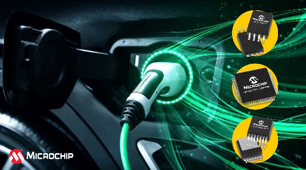
A great example of this type of product was Microchip’s new On-Board Charger (OBC) solution. The charger shows the sophistication and complexity of today's power solutions by basing the control system around one of the company’s dsPIC Digital Signal Controller (DSC) devices, which combines the features of a microcontroller and a DSP. Being adept at developing power circuits is no longer all that is required to design products like the OBC, embedded systems experience is just as necessary. As part of the OBC offering, Microchip also provides fully-featured software, which allows the customers to tune the design to their own requirements, rather than start writing the software from scratch. Although not removing the need for embedded specialists completely, the hardware/software combination definitely reduces how much effort is required.
The OBC was developed to showcase a range of Microchip products. It increases system efficiency and reliability by combining the company’s dsPIC33 DSC’s advanced control functions, with the MCP14C1 gate driver’s high-voltage reinforced isolation and the mSiC MOSFETs’ reduced switching losses and improved thermal management capabilities. The OBC design also contains other Microchip products, such as communication interfaces, security, sensors, memory and timing.
The flexible programmable solution comes with ready-to-use software modules for Power Factor Correction (PFC), DC-DC conversion, communication and diagnostic algorithms. The software modules in the dsPIC33 DSC are designed to optimize performance, efficiency and reliability, while offering flexibility for customization and adaptation.
Here main components in Microchip’s OBC solution are:
• The AEC-Q100 qualified dsPIC33C DSC with high-performance DSP core, high-resolution PWM modules and high-speed ADCs, making it optimal for power conversion applications. It is functional, safety ready and supports the AUTOSAR ecosystem.
• The AEC-Q100 qualified MCP14C1 isolated SiC gate driver comes in SOIC-8 wide-body package with reinforced isolation and SOIC-8 narrow-body with basic isolation. The MCP14C1 is optimized to drive mSiC MOSFETs via Undervoltage Lockout (UVLO) for VGS = 18V gate drive split output terminals, simplifying implementation and eliminating the need for an external diode. Galvanic isolation is achieved by leveraging capacitive isolation technology, which results in robust noise immunity and high Common-Mode Transient Immunity (CMTI).
• The mSiC MOSFET in an AEC-Q101-qualified D2PAK-7L XL surface mount package with five parallel source sense leads to reduce switching losses, increase current capability and decrease inductance. This device supports 400V and 800V battery voltages.
Microchip has also published a white paper that provides more information about how this OBC solution can optimize a design’s performance and speed up its time to market.