Click image to enlarge
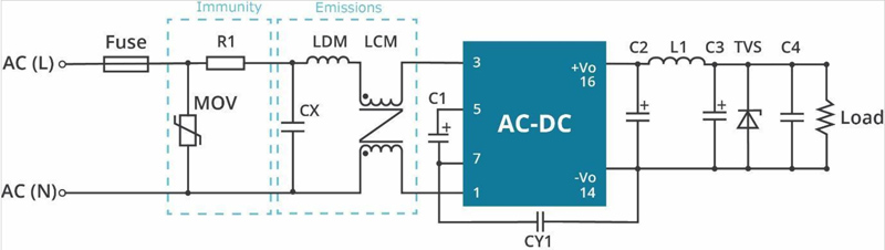
Figure 1: Reference design to meet Class B emissions and Class IV immunity from CUI Inc’s PBO-15C datasheet
Electrical and electronic systems generate electromagnetic fields that can interfere with other electronic products unless steps are taken to avoid it. All electronics products must demonstrate that they conform to standards regarding electromagnetic interference (EMI) and electromagnetic compatibility (EMC).
The sources and paths of EMI can be difficult to analyze, and new designs often fail EMI/EMC tests, potentially leading to costly production delays. Having a basic grasp on the components inside an EMI filter will help designers understand what needs to be done to meet their EMC requirements.
Where Things Can Go Sideways
Between the lack of a simple formula for calculating emissions and the complexity of applicable regulations, it is easy to arrive at an EMI filtering solution that results in test failure.
For example, a designer can select a capacitor and use it in several different places within a single design, only to discover that EMI/EMC regulations bar the use of that particular type of capacitor in a single instance – such as an X-cap or Y-cap.
The Peril with Reference Designs
Following reference designs alone cannot replace an understanding of EMI fundamentals when troubleshooting filter values. Modifications to internal filters in power supplies, integrated connector modules (ICM), or discrete magnetic components such as common mode chokes (CM) and differential mode (DM) chokes are often required.
Circuit Protection Components
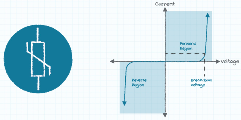
Metal oxide varistor: MOV’s are typically included in the EMI filter to meet immunity requirements. They are placed across input terminals and often from line and neutral to ground to absorb voltage transients which may come from the input voltage source. A MOV has high impedance during normal operation and becomes low impedance when the rated voltage is exceeded, clamping the voltage to protect the circuit. MOV’s fail short and an input fuse should always be placed between the MOV and the input power source.
EMI Filter Components
Differential mode choke: A DM choke is paired with a capacitor to create a low pass filter and prevent undesired differential mode noise on the input conductors from reaching an external receptor. The saturation current specification for this inductor must be great enough to tolerate the maximum input current during normal operation.
Common mode choke: A CM choke has a high impedance for common mode currents and low impedance for differential mode currents. CM chokes contain a pair of coupled chokes, one for each power or signal and return line, and are wound such that flux generated by differential currents cancel and flux from common mode currents sum. The common mode choke should be chosen, in addition to inductance, based on voltage and saturation current.
X safety class input capacitor: This type of capacitor is placed across input power lines and serves to shunt differential noise so the noise does not continue to the external voltage source. This capacitor should be of X safety class construction. In the event of a failure, X-class capacitors are designed to fail-short, which should cause a fuse or other overcurrent device to open. These capacitors are chosen, in addition to capacitance, by rated voltage and peak voltage.
Y safety class isolation capacitor: This type of capacitor is typically placed from line or neutral to earth. It can also be found between the input and the output. In both locations the capacitors’ purpose is to filter out common mode noise. Because of the danger a short circuit would pose given the earth connection, Y-capacitors are designed to fail open.
Click image to enlarge
Figure 2: Metal oxide varistor schematic symbol and voltage-current relationship
EMI and EMC standards
International standards bodies have developed multiple standards for EMC that define the levels of EMI allowable. EMI/EMC standards all encompass the fundamental concept of “do no harm” – no product should interfere with nearby systems.
Click image to enlarge
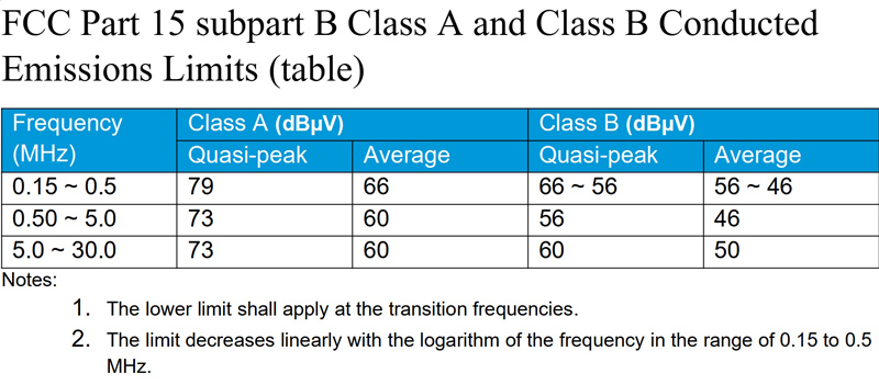
In the United States, FCC Part 15 pertains to nearly all modern electronics and has multiple sub-sections that apply to different categories of radio frequency emitting devices. Subpart B pertains to unintentional radiators and typically power supplies. Within this subpart applications are divided into Class A for industrial and business environments, and the more stringent Class B for home environments. Assuming which part of the standard applies to your design is a common path to EMI/EMC test failure.
Outside the United States different standards apply, such as those set by the International Special Committee on Radio Interference (CISPR) that cover a variety of applications. For example, CISPR 32 and CISPR 35 both apply specifically to multimedia equipment, addressing EMI emission and EMI immunity, respectively.
Test labs
Many companies provide EMI/EMC test services to identify failure points or performance shortfalls.
The following is offered as an example of the complexity of EMI conformance and the interpretation of test results.
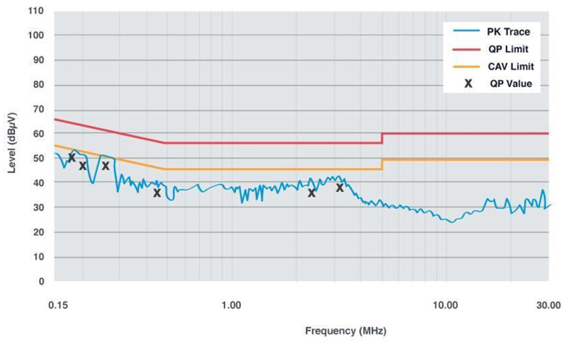
The graph below shows a product whose emissions (the blue line) remain below recommended limits (the red and magenta lines).
Click image to enlarge
Figure 3: Emissions versus frequency - The blue line shows the peak measurement of the emissions (Y-axis, in decibel micro-volts [dBµV]) versus frequency (X-axis, in MHz). The red line is the quasi-peak limit and the magenta line is the average limit. Xs (1-6) are measurement points
Further analysis will reveal if the target margins have been met and, if not, will help determine the attenuation required to achieve those margins.
The numerical values on the table below provide finer detail. Again, while emissions remain within recommended limits, at some frequencies they may be close to or perhaps even below unacceptable margins.
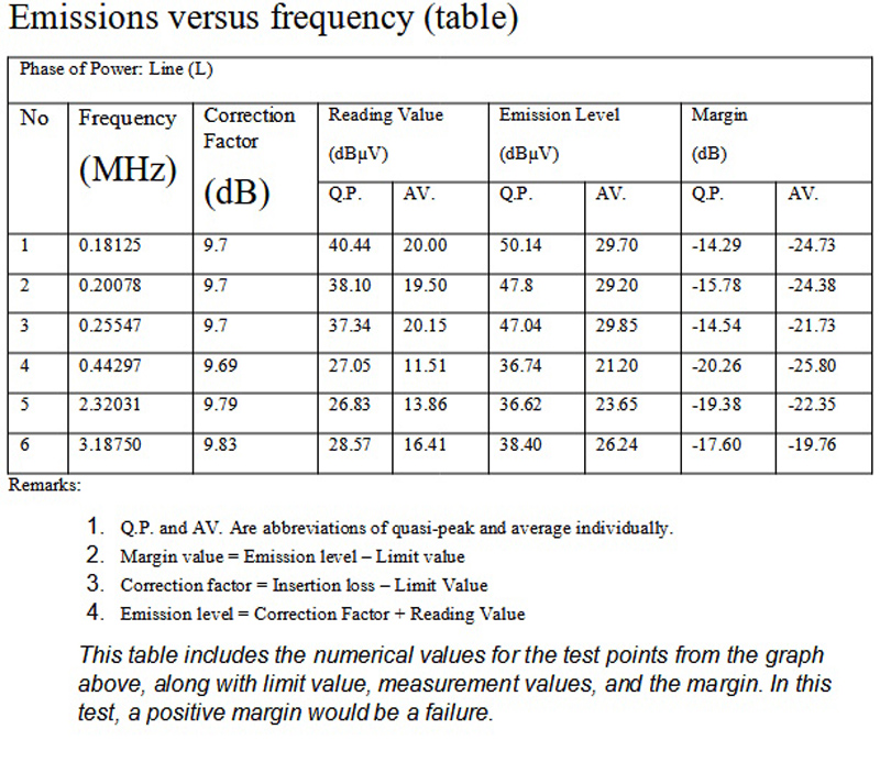
Click image to enlarge
Given the test margin, you can calculate the difference, giving you a number equal to the attenuation required.
For example, if
desired margin = -10dBuV, test = +5 dBuV,
Required attenuation = -10dB – 5 dB = -15dB
Note that this value is for a single data point at a single frequency. A filter solution will have to provide the correct attenuation at all frequencies.
There are two basic options for solving an EMI design problem.
Apply integrated component EMI filters. Integrated filters simplify the design process at the potential expense of optimization. Integrated filters can be found for both signal level and power filters. CUI has EMI filters such as this for power applications. This kind of filter is accompanied either by a graph of the attenuation vs. frequency or an attenuation and frequency range (as this one does). This one has 20dB attenuation from 150kHz to 1GHz. Note that this one would be a good candidate for the example above.
Design a discrete filter. For designs that have more specific size or performance requirements, a discrete filter may be the better option. This solution can be the most optimal and lower cost long term, but can increase development time.
Understanding this information and the components that affect each result is necessary to properly modify the filter and/or understand what options are available and how that may impact the final design.
 PDF
PDF