Gallium nitride (GaN) field-effect transistors (FETs) have revolutionized power electronics with their superior performance characteristics. However, like all power devices, heat management remains critical
Figure 1: Cross-section view of GaN devices mounted on a PCB in a half-bridge configuration without a heatsink and the equivalent thermal circuit
Effective thermal design at the printed circuit board (PCB) level can substantially improve cooling without the need for a heatsink. This article presents simple thermal management guidelines maximizing heat conduction from the GaN FETs to the environment using just the PCB and optimizes thermal performance without the use of a heatsink.
Understanding Heat Flow in GaN Devices
When in operation, power electronic devices dissipate heat primarily through two paths: the PCB and the device’s case or backside. The thermal resistances encountered along these paths determine the junction-to-ambient thermal resistance (RθJA), which significantly impacts thermal performance. Internal device construction dictates initial resistances, while PCB design dictates subsequent resistance pathways. Thus, optimizing PCB design parameters like copper layout, thickness, and via configuration is pivotal for effective thermal management.
Figure1(a) shows how heat flows from two GaN devices mounted on a PCB in a half-bridge configuration. The equivalent thermal circuit of this configuration is shown in Figure 1(b). The collective thermal resistances in this system reduce to a single equivalent thermal resistance of RθJA.
Key PCB Design Considerations for Thermal Optimization
The various PCB design characteristics that have thermal characteristics are board area, copper area, copper thickness, vias, and device proximity. Each independent characteristic has a thermal performance and an impact on the electrical system.
1. Board Area
One of the main characteristics that influences heat transfer to the ambient is the area of the PCB. Larger PCBs provide more surface area for heat dissipation. However, the thermal benefits plateau as board size increases beyond a certain threshold. Nonetheless, the PCB must be large enough to be able to dissipate the devices’ heat losses, with a general rule of 15 cm2 in area for each watt dissipated resulting in about a 40°C temperature rise.
2. Copper Trace Width and Plane Area
Copper serves as the primary medium for heat conduction and dissipation. The width and plane area of copper traces directly influence thermal performance:
Click image to enlarge
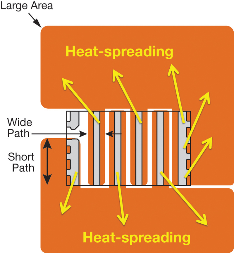
- Maximizing Thermal Spread: Wider copper traces and larger copper planes reduce localized heat build-up. Narrow traces trap heat, whereas wider traces and connected planes enhance thermal dissipation. Figure 2 shows the design of a layer that maximizes the area of the copper planes around the device with wider traces connected to large areas of copper, which in turn keeps the thermal resistance from junction to ambient low.
- Layer Thickness: Increasing copper thickness for low electrical resistance also benefits thermal resistance and provides a high thermal-conductance medium at each layer in the PCB. For example, doubling copper thickness from 1 oz to 2 oz reduced RθJA by 21%. However, benefits diminish beyond 2 oz due to manufacturing challenges and diminishing returns.
3. Thermal Vias
The insulating dielectric layers of a PCB have low thermal conductivity which results in a high thermal resistance from the device to the copper layer on the opposite side of the PCB. However, the inner and bottom layers of the PCB can still be designed into the thermal solution by connecting them to the top layer with highly conductive thermal vias.
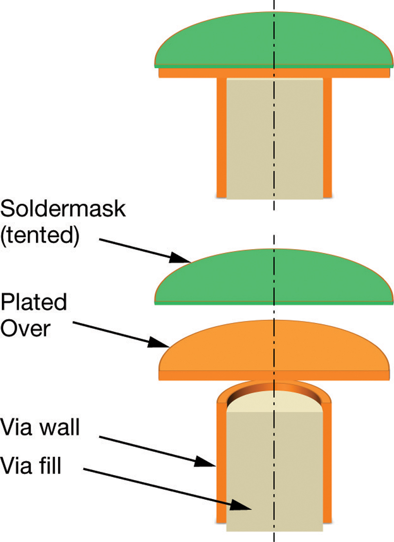
Vias should be located under or adjacent to the device. For vias directly beneath the device, IPC4761Type VII “via-in-pad-plated-over” (VIPPO) configurations, as shown in Figure 3, meet design requirements and prevent solder drainage.
Click image to enlarge
When comparing different configurations; using the no via case as a baseline, a layout using adjacent vias showed a 22% decrease in RΘjma , while the under-bump design results in a decrease of 33%.
4. Device Separation
Typical half bridge configuration GaN FET layouts require close proximity between the two devices to ensure lowest loop inductance. However, minimizing heat flux exchange between adjacent devices can lower their combined thermal resistance. Spacing out devices, such as moving the bus capacitor to between the the FETs, reduces RθJA by approximately 5%, with minimal impact to loop inductance and thus has no impact on electrical performance.
Managing Joule Heating Effects
Heat is not only generated within the GaN device. The flow of current through the copper in the board, particularly in thinner connections with increased current density, also results in power losses that generate heat. The heat that is produced through electrical current flow is known as joule heating. Joule heating surrounding the parts can be reduced using the following principles:
- Wider Pads: Expanding copper pads reduces current density, mitigating joule heating. In the regions with the highest current densities, the joule heating decreases by about three to five times as much when the copper pad width is doubled.
- Vias for Current Sharing: Adding vias allows current to distribute across multiple PCB layers, further reducing top-layer heating.
Combined Thermal Techniques: Case Study
Comparative analysis of two PCB configurations underscores the impact of combined thermal optimization. When combining the techniques outlined in this article, it is possible to reduce RθJA by close to 30% when compared to the baseline with none of the techniques used.
-
Baseline Board:
- 0.5 oz copper thickness
- 4 layers
- No thermal vias
- Adjacent devices
-
Optimized Board:
- 2 oz copper thickness
- 4 layers
- Under-bump vias
- FETs separated using center bus capacitor configuration
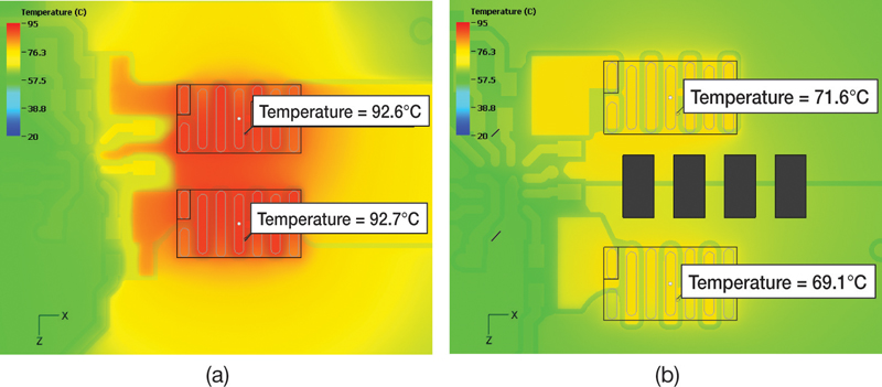
Figure 4 shows these two board designs and their thermal simulation results.
Click image to enlarge
The optimized design reduced RθJA by over 35% and operating temperatures by more than 20°C under natural convection. Adopting these techniques to the board layout not only can reduce RθJA, but also comes at little to no additional cost in manufacturing of the PCB.
Practical Guidelines for Engineers
To achieve efficient PCB-based cooling for eGaN FETs, power engineers should:
- Maximize Copper Utilization: Increase trace widths and plane areas, focusing on the layer directly soldered to the device.
- Incorporate Thermal Vias: Use IPC4761 Type VII vias either under the device or adjacent to it.
- Optimize Device Layout: Separate heat-generating devices where possible.
- Select Appropriate Copper Thickness: Balance manufacturing constraints with thermal benefits, targeting 2 oz layers where feasible.
- Design for Joule Heating Mitigation: Use wider copper pads and add vias to spread current paths.
Conclusion
By employing these PCB design strategies, engineers can effectively dissipate heat from GaN FETs, achieving superior thermal performance without added cost or complexity. These techniques not only improve device reliability and efficiency but also support compact, high-power-density applications essential to modern power electronics systems. Incorporating these best practices will help engineers unlock the full potential of GaN technology.