Author:
By: Susheel Badha, Principal Engineer, Kevin Tomas Manez, Principal Engineer, Filippo Rosetti, Application Manager: All at Infineon Technologies
Date
08/21/2024
 PDF
PDF

Click image to enlarge
Figure 1: Battery backup unit (BBU) architecture in data centers
The rapid growth of data centers due to increased AI demand has amplified the need for innovative, compact, and energy-efficient power solutions. A critical component of these solutions are Battery Backup Units (BBUs), whose power ratings must scale up to meet the growing power demands, reaching up to 12 kW, without expanding their physical size. This is a challenge as battery sizes are increasing, leading to a reduction in space for DC-DC converters.
Possibilities of improving BBU ratings
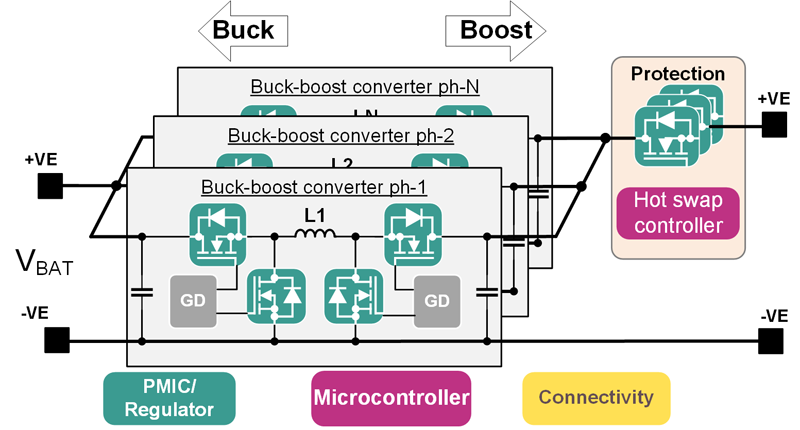
Presently, almost all BBUs use a 11S/12S configuration which results in a high current drawn of about ~420 A at 10 kW. As a result, multiphase DC-DC converters are inevitable. But synchronous buck-boost converters are hard-switching topologies with dominant switching losses that only get worse with parallel MOSFETS. Clearly, this results in a corresponding increase in the system losses, adversely affecting the efficiency of the system and bringing down the data center’s ROI.
So, an increase of the BBU voltage rating is inevitable to address these challenges. The BBU’s battery configuration (the number of cells in series) is limited by SELV requirements, which dictates an output voltage ≤60 V DC. This translates to 14 or 15 individual cells in series with 4 V/cell max. These configurations are called as 14S or 15S respectively, and have an operating range as 36 V (VBat_min) to 60 V (VBat_max). This satisfies increased voltage needs. Now, when this configuration is operational at the minimum voltage, it would draw currents that are 20-25 percent lower of ~300 A at 10 kW. This provides the benefit of a significantly lower bus-bar conduction loss. But on the flip side, the upper and lower limits of the battery’s operating range are higher and lower than the bus voltage (48 V, VBUS). This warrants the need for both step-down and step-up conversion of the voltage during the charging and discharging of the battery, from and in to bus, respectively. A state-of-the-art four-switch full-bridge buck-boost converter that has to be used here suffers from low efficiency and power density, and high power losses, BOM cost, and quantity. So, there is a need of a new converter topology that offers a higher power density and efficiency at a lower or similar BOM cost as the four-switch buck-boost converter to adapt 14S/15S battery configurations in the BBU.
Click image to enlarge
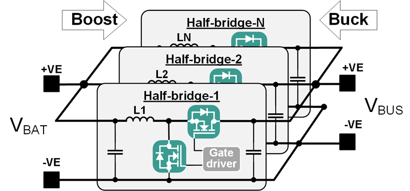
Figure 2a: Half-bridge configured buck or boost converter
Click image to enlarge
Figure 2b: Buck-boost converter
Differential Power Current-Fed Step-Up Step-Down (DP-CF-SUSD)
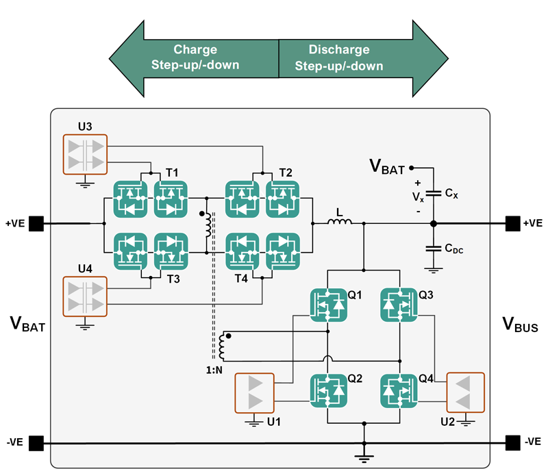
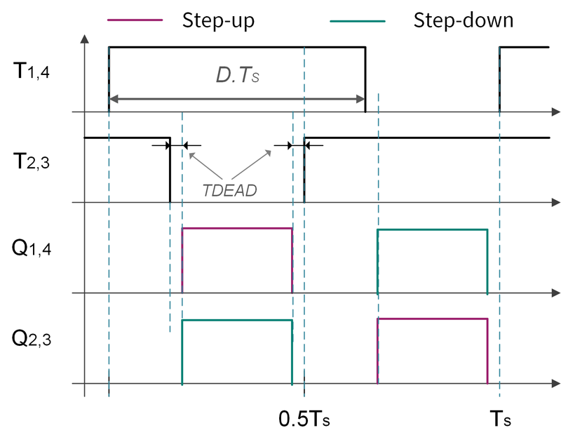
The essence of Infineon’s novel approach to improving the BBU’s performance – a differential power processing converter topology with a current-fed full-bridge that can perform step-up and step-down conversion (Differential Power Current Fed Step-Up/-Down, or DP-CF-SUSD) as shown in Figure 3.
Click image to enlarge
Figure 3a: Differential-Power Current-Fed Step-Up Step-Down (DP-CF-SUSD)
topology
Click image to enlarge
Figure 3b: its PWM signals during operation
DP-CF-SU-SD outperforms existing solutions in efficiency, power density, and cost-effectiveness, while maintaining power scalability flexibility. It consists of a MOSFET full-bridge in parallel with the 48 V DC bus and a current-fed MOSFET full-bridge in series with the bus and the battery.
To facilitate both step-up and step-down operation in both power flow directions, the current-fed full bridge (T1-T4) requires reverse blocking voltage capability, which is achieved by implementing the MOSFETs in a back-to-back configuration. A transformer (X) with a turns ratio of N:1 interconnects the two full-bridges for energy transfer. The inductor (L) serves as an energy storage element, like in traditional DC-DC converters.
The operating principle of the DC-DC converter is based on generating a modulated DC voltage (Vx) across the current-fed full-bridge, which can vary between -VDC/N and +VDC/N depending on the duty cycle (D). The gate signals controlling this operation are illustrated in Figure 3. The current-fed full-bridge is driven by two complementary signals, each controlling a diagonal pair of MOSFETs (T1, T4 and T2, T3), with a 180° phase shift and a duty cycle (D) that can range from 50 percent to 100 percent.
During the step-down mode, the Q1-Q4 full-bridge functions as a synchronous rectifier, with the corresponding diagonal pair of MOSFETs turned on according to the transformer polarity convention. Conversely, in the step-up mode, the opposite diagonal pair of MOSFETs in the Q1‑Q4 full-bridge is switched.
Impact of transformer turns ratio on converter performance
Click image to enlarge
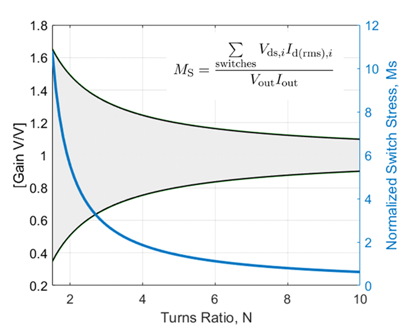
Figure 4: Minimum and maximum voltage gain and MOSFETs stress factor vs turns ratio
The input-to-output voltage gain of the DC-DC converter depends on the duty cycle (D) and the transformer turns ratio (N:1). The impact of N:1 on the converter gain is illustrated in (Figure 4), which shows the minimum and maximum achievable gain. As the turns ratio increases, the input and output voltage ranges narrow, resulting in a more limited operating range. However, to achieve optimal performance, a larger transformer turns ratio is desirable.
Examining the turns ratio’s impact on converter performance is crucial for fully exploiting the advantages of the topology.
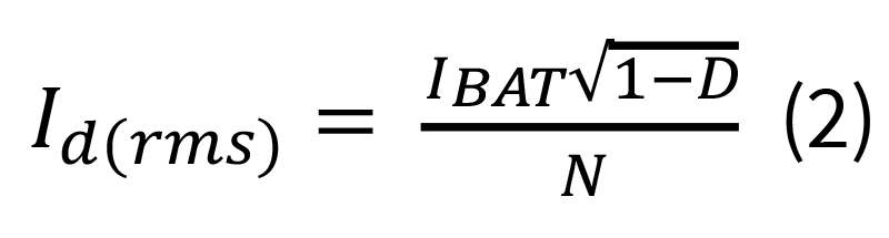
Firstly, the MOSFETs in the current-fed full-bridge (T1-T4) are required to block a voltage of |VDC/N| (Equation 1) and not all of VDC or VBAT. This enables the use of lower voltage class devices, resulting in a better RDS(on)*A and more effective exploitation of the non-linear ON resistance vs voltage dependency of semiconductors. Meanwhile, although the MOSFETs Q1-Q4 must block the entire DC bus voltage, only a portion of the current flows through them, as described by Equation 2, leading to lower power loss and heat generation.

Additionally, the voltage excitation of the inductor is N times lower compared to traditional topologies and the equivalent inductor frequency is two times the switching frequency. This leads to a large reduction of the inductance required and thus achieves a substantial improvement in efficiency, power density, and transient response.
Unlike conventional topologies, the power flows from the input to the output during all switching states, largely reducing the input and output capacitance. Around the nominal operating point, where the duty cycle approaches 100 percent, the converter topology behaves nearly like a short-circuit input-to-output through the inductor (L).
Click image to enlarge
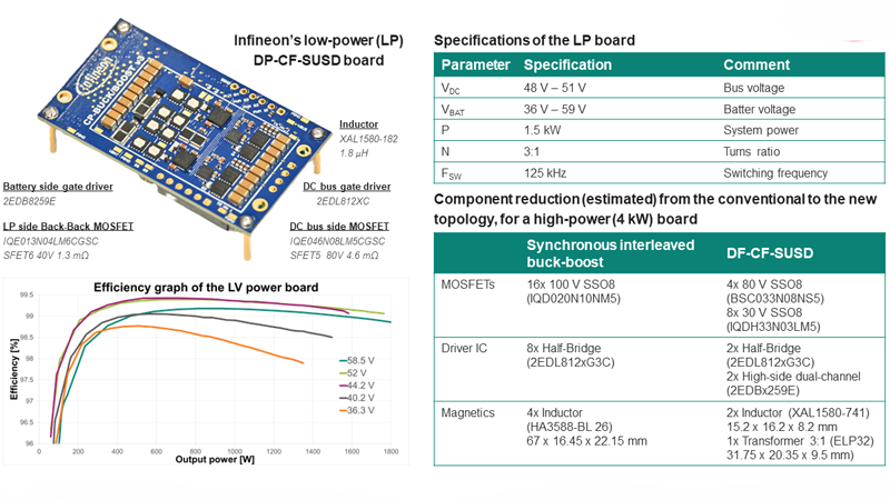
Figure 5: A low-power (LP) DP-CF-SUSD board, its specifications, and its efficiency measurement; component reduction estimation for a high-power (HP) board
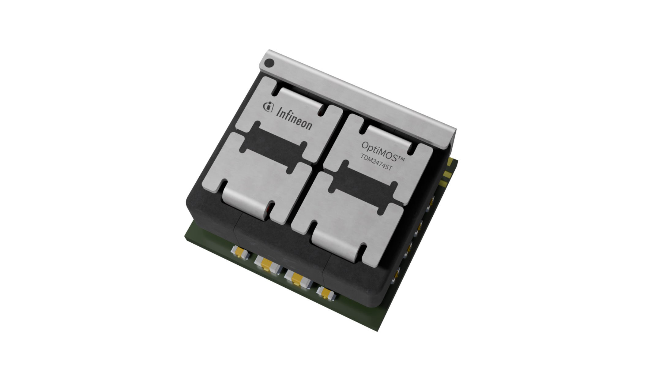
During internal lab-testing for the conversion efficiency of the topology, Infineon’s newly-developed low‑power board based on PQFN 3.3x3.3 mm2 packages, reached 1.5 kW output power under all operating conditions with a peak efficiency of 99.45 percent (Figure 5). The switching devices used are low-RDS(on) OptiMOS™ 40 V source‑down MOSFETs with EiceDRIVER™ 2EDB gate drivers and OptiMOS™ power MOSFETs 80 V with EiceDRIVER™ 2EDB gate drivers. The turns ratio selected for this board is 3:1, and the switching frequency is 125 kHz. It must be noted that this new converter topology requires an inductance as low as 1.8 µH.
Based on the results, specifications, and observations of the low-power (LP) board rated for 1.5 kW, we estimated the same for a high-power (HP) board rated for 4 kW. We also compared a conventional buck-boost converter against the DP-CF-SUSD to check for component reduction, for an operating frequency of 140 kHz. The results (figure 5) show that the power density of the conventional topology is ~73 percent lower than the novel topology, and yet the BOM cost for the novel topology is ~43.5 percent less than the conventional topology, resulting in a 76 percent decrease in PCB footprint.
Clearly, the new ultra-high-power density topology from Infineon will go a long way in increasing the ratings of the BBUs in data centers, without needing an increase in size. This results in savings on cost and space, and combined with the scalability offered, DP-CF-SUSD is well placed to address the challenges of 11S/12S configurations. Click or scan the QR code to learn more about the new DP-CF-SUSD or to explore all of Infineon’s offerings for data centers. Stay tuned for upcoming designs.