Date
02/28/2025
 PDF
PDF
When designing a robust and high-density power architecture for space systems like satellites, engineers must grapple with a variety of design complexities, including limited board space, power dissipation requirements, and damaging radiation effects. To address these challenges and reach peak operational performance and reliability, it becomes necessary to explore new radiation hardened (RH) MOSFET designs over conventional options. Learn about superjunction technology, understand its implications on RH power MOSFET performance, and identify how they can help create high-efficiency power systems in space.
To go beyond the silicon limit established by conventional planar gate vertical double-diffused power MOSFETs (VDMOSFET), designers implanted doped semiconductor pillars in a MOSFET’s epitaxial layer (a layer also referred to as the device’s “active” region where the power stage current will flow when the device is operating). Figure 1 illustrates the key differences between both power MOSFET styles using the N-channel option. These pillars possess a charge concentration that opposes the epitaxial region to achieve “charge-balancing” - reducing the amount of electrical stress a power MOSFET experiences when given a drain-to-source voltage (VDS) bias. As a result, manufacturers could more heavily dope the active region of a superjunction power MOSFET (SJMOSFET) to reduce the device’s drain-to-source resistance RDS(on) without compromising the device’s voltage blocking capabilities. With enhanced conduction abilities, smaller die sizes could be developed for SJMOSFETs - reducing other component characteristics like parasitic capacitances, gate-charge requirements, and switching times that mainly depend on device size. The first SJMOSFETs were released in the late 1990s for commercial, terrestrial applications. These superjunction columns were recently mixed into a device designed to withstand harmful radiation from various sources to produce RH variants. Several metrics will now be examined to understand how a RH SJMOSFET offers superior performance over conventional RH VDMOSFET counterparts.
Due to a richly doped epitaxial layer, the RH SJMOSFET family enjoys a significant improvement in its safe operating area (SOA) over legacy RH VDMOSFET generations. For example, Figure 2 illustrates the difference in SOA between several RH P-Channel SJMOSFETs (denotated as R9) vs several RH P-Channel VDMOSFETs (denotated as R5). As evidenced by the SOA plots, superjunction technology enables RH SJMOSFETs to deliver superior RDS(on) over RH VDMOSFETs with the same active area and voltage rating. Consider how these RH SJMOSFETs compare to their conventional equivalents in load-switching or active-Oring applications for critical DC busses on a spacecraft. With a RH SJMOSFET’s enhanced current carrying capacity, these devices could be placed in high-current power distribution systems or enable more efficient solutions that legacy RH VDMOSFET options could not support (one could opt to use a larger option instead, but the valuable size and weight tradeoff may be untenable for space power systems). Next, let’s examine how RH SJMOSFETs compare with legacy generations when switching.
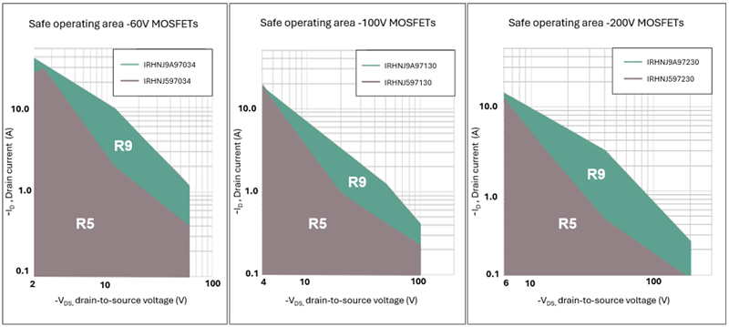
Click image to enlarge
Figure 2: Despite employing the same package (SMD-0.5 housing), these three RH SJMOSFETs show significant increases in SOA vs RH VDMOSFETs
In switch-mode power supplies (SMPS), high-frequency switching losses tend to dominate over conduction for many types of power MOSFETs. These switching losses are tied to the size of the three parasitic capacitances associated with a power MOSFET: output capacitance (Coss), input capacitance Ciss , and reverse transfer capacitance (Crss). Larger MOSFETs generally have greater parasitic capacitances. For SJMOSFETs, they have a reputation for possessing a nonlinear (Coss), . The superjunction pillars drive this nonlinear behavior of (Coss), because increased VDS biases will induce stronger electrical fields onto the pillars; reducing the effective (Coss)the pillars contribute as their population of embedded charges scatter Figure 3 shows how (Coss), Ciss,and Crssfora 100 V N-Channel RH SJMOSFET (R9) and a larger die size 100 V N-Channel RH VDMOSFET (R6) change with VDS. Despite the R9 active area being 75 % smaller than the R6, the difference in RDS(on) does not share the same discrepancy (34 mΩ vs 10 mΩ respectively). Notice in Figure 3 the large reduction in (Coss)and Cissthe R9 enjoys over the R6 without significantly conceding conductivity – enabling higher efficiencies for SMPS of many topologies. Legacy RH VDMOSFETs do not offer a similar opportunity. To provide a complete description of the RH SJMOSFET generation, their radiation performance will be addressed next.
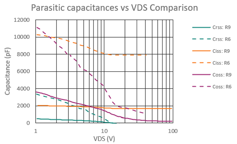
Click image to enlarge
Figure 3: A typical comparison of parasitic capacitances for a RH SJMOSFET (R9) and an equivalently rated RH VDMOSFET (R6)
An RH power MOSFET is specifically designed to withstand the damaging effects of heavy ion radiation like total-induced radiation (TID) degradation or Single-Event Effects (SEE), unlike power MOSFETs designed for terrestrial applications, if used in space, can become irreversibly damaged resulting in the crippling of a satellite’s power system. Let’s examine a common concern for high-power electronics in space: a destructive Single-Event Burnout (SEB) can start to manifest when a heavy ion, possessing a high linear energy transfer (LET) value, passes through a biased (but inactive) power MOSFET’s epitaxial layer-inducing a large concentration of charge to travel within the device. This movement of charge can incidentally activate a parasitic bipolar transistor junction (BJT) found at the intersection of a power MOSFET’s source, base, and epitaxy regions (refer to Figure 1 again) – allowing a high power-dissipating runaway current to grow throughout the device. High voltage power MOSFETs are especially vulnerable to overheating as they are typically lightly doped. With all the component benefits superjunction technology provides to the RH SJMOSFETs, it is common for them to also enjoy greater integrity against radiation over legacy RH VDMOSFET alternatives. Remember, the superjunction segments allow an R9 device to be more richly doped than its legacy counterparts. Thus, an RH SJMOSFET can experience greater amounts of incidental current propagation from an ion strike, subsequently recover, and more likely avoid a SEB. Figure 4 compares the SEE-SOA and Post-TID electrical characteristics of a similarly sized 100 V RH SJMOSFET and 100 V RH VDMOSFET to exemplify the improved radiation-survivability a RH SJMOSFET enjoys. Consider how the 100 V RH SJMOSFET does not require VDS derating when subjected to a high LET like 89.8 MeV * cm2 /mg
whereas the 100 V RH VDMOSFET cannot safely exceed 50 V. For systems requiring bus voltages greater than 50 V, a higher voltage RH VDMOSFET would have to be selected (thus comprising conduction efficiency) if high-LET heavy ions are expected to be present in the mission. In addition, Figure 4 shows how a RH SJMOSFET does not significantly degrade for various levels of TID when compared to the RH VDMOSFET. Frequently, a space power system designer will be able to find a drop-in RH SJMOSFET replacement for a legacy RH VDMOSFET option through a common package selection.
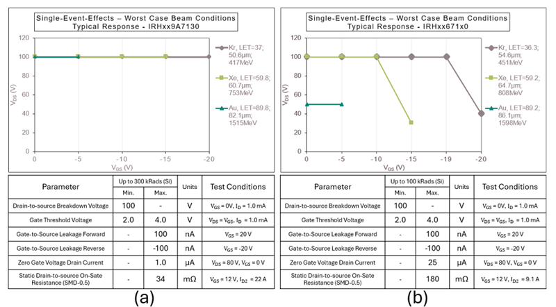
Click image to enlarge
Figure 4: SEE-SOA and Post-TID electrical parameters for (a) 100 V RH SJMOSFET and (b) 100 V RH VDMOSFET
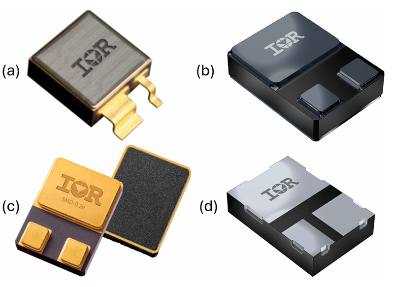
Many RH power MOSFETs have been available in several surface-mount-technology (SMT) packages including the SMD-2, SMD-0.5, and SMD-0.2 for years. When mounted to PCBs using materials like FR-4 or polyimide and subjected to extreme thermal cycling conditions like the military range of -55 °C to 150 °C, these legacy packages show significant solder joint fatigue and hermeticity loss. As a result, these packages would require carriers to be safely mounted – adding additional package resistance and inductance. New package technologies have been pursued to mitigate environmental effects to properly support the power system performance boost offered by RH SJMOSFETs. For example, the large size of the SMD-2 makes this package particularly vulnerable to damaging thermal stress effects. A new, alternative option like the 35% smaller SupIR-SMD with its wide, curved package leads offers thermal stress relief (no need for a carrier now) and the same high current carrying capabilities. Smaller package options like the SMD-0.5 and SMD-0.2 can also experience significant solder joint cracking; improved variants like the SMD-0.5e and SMD-0.2e are built with more ceramics and possess high conductivity, mixed-material pads to transfer heat more efficiently. With smaller die sizes enabled by RH SJMOSFETs, the hermetic, ceramic package SMD-0.1 (measured at 5.72 x 3.94 x 1.96 mm^3) was developed to ensure minimal board space is taken.
Figure 5 shows these four advanced package concepts best suited to maximize the performance RH SJMOSFETs have to offer.
Click image to enlarge
Figure 5: Shown here are four new space-grade, hermetic packages: SupIR-SMD (a), SMD-0.5e (b), SMD-0.2e (c), SMD-0.1 (d)
As the capabilities of spacecraft expand with the addition of new systems like edge computing and the implementation of power-hungry AI, rapid advancements in power system density and efficiency are essential. Coming in VDS classes from – 200 V to 650 V, several die sizes, and package options, the MIL-PRF-19500 JANS R9 and ESCC-500 RH PowerMOS product families with N-Channel and P-Channel options have proven flight heritage to support many space applications.
To learn more about Infineon Technologies IR HiRel (IFX IR HiRel)’s R9 and RH PowerMOS products, please visit https://www.infineon.com/cms/en/product/high-reliability/space/power/rad-hard-mosfets/


