press x to close
Author:
Annika Frankemölle, Alexander Lang / Editor: Gerhard Stelzer, Würth Elektronik
Date
03/31/2025
 PDF
PDF

Figure 1: Reference schematic of a buck converter Vin = 24 V; Vout = 5 V
Increasing current densities and short switching times in MOSFETs are placing ever greater stress on the dielectric strength of inductors. Molded inductors with a distributed air gap based on iron powder enable high inductance values in the smallest of spaces and thus increase the power density. A new test concept is designed to precisely determine the maximum permissible operating voltage.
Inductors play a decisive role in influencing the current rise in electrical circuits. The current resulting from the applied voltage induces a magnetic field that counteracts the current, thus controlling and limiting the current increase. When selecting a suitable coil for an application, the inductance value and the maximum currents generated must therefore be considered, as they play a central role in the desired function, e.g. in a switching regulator.
In the past, inductors in electrical circuits were made with both iron powder and ferrite cores. For shaped cores, a coil former was used to stabilize the wire windings. The windings can be applied directly to toroids, as they are insulated with a coating. The epoxy coating applied to toroids served as protection against corrosion and moisture and to indicate permeability.
The selection of the insulating layer on the enameled copper wire was primarily based on the temperature class and not on the dielectric strength, as the enameled wires used can usually withstand several thousand volts.
Dielectric strength of molded inductors
However, manufacturing processes have changed in recent years with the increasing popularity of molded inductors based on fine iron powder with a distributed air gap. The powder used as core material consists of pure iron or iron powder alloys, such as mixtures of nickel, manganese or zinc, and is pressed around the enameled copper winding under high pressure with insulating synthetic resin as a binder. Thanks to the continuous optimization of the production process and the material composition, it is possible to achieve a high permeability to realize high inductance values in the smallest possible installation space. This must be combined with the maximum possible current carrying capacity. As a result, the power density per volume can be continuously increased.
To constantly increase the load capacity of the coil with the smallest possible volume, the proportion of iron powder or iron alloys in relation to the insulation of the binder has been continuously increased, so that the distance between the individual grain sizes has become smaller and smaller.
This reduction has meant that today, when selecting a coil for an application, the voltages applied to the inductance in a DC/DC converter must be taken into account, as the lower insulating material content in the powder core reduces the dielectric strength of the material and therefore a high operating voltage can lead to the failure of the entire application.
As an example of the changing market conditions in electronics, the voltage drop across a coil in a buck converter (Figure 1) is considered below. At the moment of switching on, between 24 and 36 V are present at the input. The insulation of the powder particles must therefore be able to withstand 36 V permanently.
Thanks to constant technical progress in the semiconductor industry, MOSFETs can now achieve high current densities and short switching times. This makes it possible to reduce the output voltage of DC/DC converters further and further.
Example: In the past, an input voltage of 48 V was gradually reduced to 12 V, then to 5 V and finally to 1.8 V. By using GaN MOSFETs in the application, however, it is possible to reduce the voltage from 48 V directly to 1.8 V with extremely low switching losses (efficiency > 90 %). If possible, tolerances in the input voltage are also considered, up to 60 V can be applied to the coil at times in the application. Such a high value was rather unusual in the past.
By using highly efficient MOSFETs, the developer therefore has the advantage of not having to regulate the voltage in steps and can therefore achieve a high-power density and better efficiency in a compact housing. This allows the entire application to be further miniaturized, which has a cost-reducing effect.
For this reason, the question of the dielectric strength of coils has become increasingly important in recent years when selecting the right inductor and will continue to play a significant role in the future.
To ensure the necessary transparency, Würth Elektronik has decided to integrate the new characteristic of insulation strength into the data sheets for all powder-based storage inductors. A modern testing concept was developed for this purpose, which is explained in more detail below.
Operating voltage and peak voltage
In its data sheets, Würth Elektronik specifies the maximum operating voltage Vop at which an inductor can be operated continuously during the application without impairing performance, risking damage or overheating the component. The operating voltage is therefore a limit value for the input voltage up to which the inductor can be reliably used in an application without irreversible damage. The maximum operating voltage of a molded inductor can be influenced by various factors. These include the inductance value, the ambient conditions or the material composition. In addition, the structure of the component can also play a decisive role. For example, the arrangement of the winding layers of the coil and the insulating materials on the copper wire can have an influence on the maximum operating voltage.
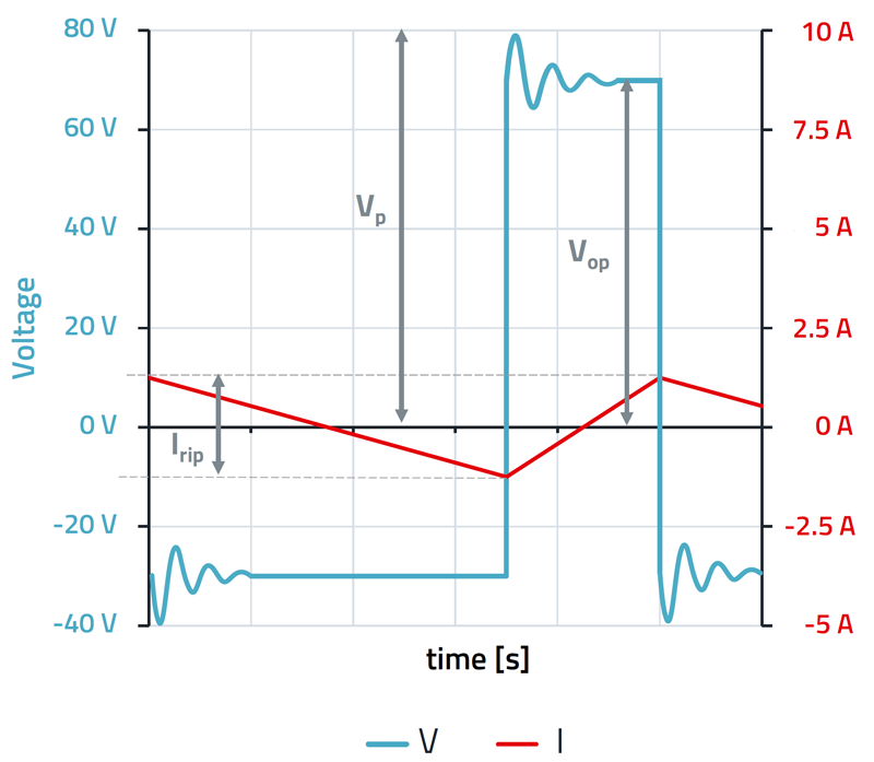
In contrast to the operating voltage (Vop), the value of the peak voltage (Vp) refers to the maximum voltage across the inductance that does not cause any damage. The peak voltage may only be applied to the coil for a short period of time compared to the total duty cycle. During the switching processes in a buck converter, for example, the voltage across the inductance briefly exceeds the maximum value of the operating voltage (Figure 2).
Click image to enlarge
Figure 2: Inductor voltage (blue) and current (red) – Delimitation of Vp versus Vop.
This is mainly due to the parasitic effects of the MOSFET and the inductance. A storage inductor used in this application must be able to withstand the short-term voltage peaks without being damaged or impairing the reliability of the circuit.
Exceeding the operating voltage
As described above, continuous optimization of the ratio between the metal particles and the binder led to a reduction in the insulation strength. But what happens when the stress becomes too high? To better understand this, it is worth analyzing the structure of a molded inductor in more detail.
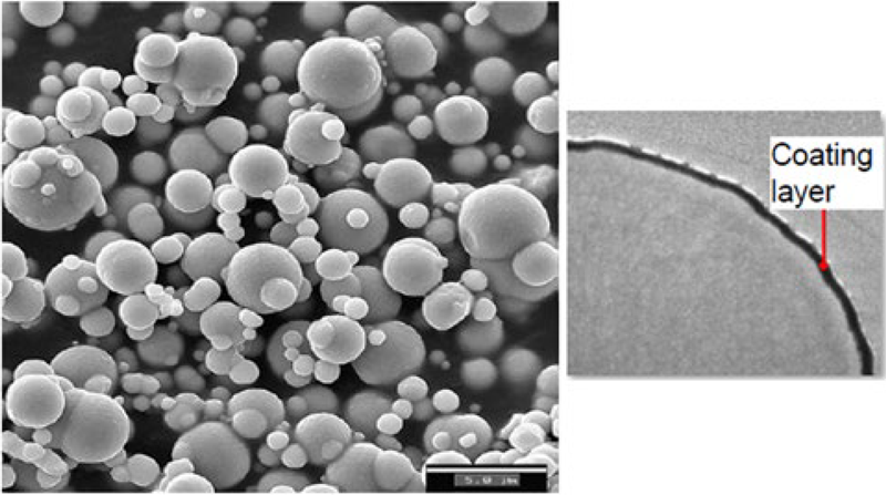
Ferrite materials are usually ceramic compounds consisting of iron oxide (Fe2O3) in combination with other metal oxides such as manganese, nickel or zinc. These materials have a crystalline structure in which the iron and other metal ions are arranged in a specific lattice form. This crystalline structure inherently prevents the free movement of electrons, which leads to non-conductive behavior. The oxide process “binds” each of these particles, protecting them from environmental influences (Figure 3).
Click image to enlarge
Figure 3: Microscopic analyze of a powder structure of a molded inductor [Zoom: 5µm]
This is a great advantage because iron begins to rust as soon as it encounters moisture and oxygen in the air and the electrical properties affecting inductance would be lost. Depending on the area of application, there are different types of oxides or manufacturing processes that lead to “passivation”, e.g. resistance to chemical influences, temperature or humidity. The thickness and material of the coating created by the manufacturing process also play an important role. Depending on the coating used, the more resistant it is to environmental influences, the less opportunity to increase power density. Reliability and electrical performance must be weighed against each other during production to determine the optimum ratio.
A second factor is the binder that holds the individual particles together after the molding process. This must also be able to withstand the environmental influences. The particle coating and binder between the particles together form a barrier between the conductive parts of the component and the connections.
If this barrier is not high enough for the voltage used in the application, a conductive path is created through the core material by flashovers between the individual metal particles. Figure 4 shows that the particles have melted together after an excessive voltage has been applied.

Click image to enlarge
Figure 4: Microscopic analyze of a melted powder structure of a molded inductor [Zoom: 10µm]
Comparative test of damaged and intact inductance
To illustrate the influence of non-compliance with the maximum voltage in a real application, a measurement setup was created. What effects can an excessively high applied voltage have on the actual application? Two identical molded inductors were used for the test setup. In one case, the insulation damage was caused in advance by several voltage pulses of over 200 V. The other coil was removed directly after production.
At first glance, there is no visible difference between the damaged and the intact component. Nor can the fault be determined by measuring the electrical properties according to the data sheet. Even after measuring the inductance and RDC of both components, the electrical properties are still within the specification. For this reason, the existing specifications in the data sheets are not sufficient.
To show the influence of a damaged component, both components were inserted into the circuit of a step-down converter with an input voltage of 18 V to an output voltage of 5 V and an average output current of 1 A (Figure 5).

Click image to enlarge
Figure 5: Test board with inductor mounted on the red PCB
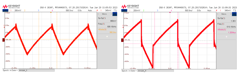
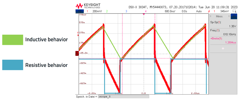
To evaluate the insulation effect, the ripple current of each coil is recorded (Figure 6). The shape of the ripple current of the damaged component has changed compared to the intact component. The reason for this is the reduced creepage distance in the core material caused by damage from the excessive voltage. Schematically, there is now a resistance parallel to the inductance (Figure 7). The new signal curve is now the combination of these two components. The behavior of the coil (green line) and the resistor (blue line) has been entered in the ripple current diagram (Figure 8).
Click image to enlarge
Figure 6: Screen capture of the ripple current, undamaged component (left) and damaged component (right)

Click image to enlarge
Figure 7: Due to excessive voltage, there is a conductive path through in the core material, which can be modelled as a resistor in parallel to the inductor
Click image to enlarge
Figure 8.: Ripple currents of the undamaged and damaged component in one diagram
The application still works: The voltage is lowered from 18 V to 5 V. But what influence does this resistor, which can be seen in the circuit diagram and the ripple current diagram, have? The answer to this question can be found by checking the self-heating of the coil. A thermal imaging camera was used to compare the temperature rise of the inductor to visualize the difference in the self-heating of the two components (Figure 9).

Click image to enalrge
Figure 9.: Self-heating recorded of the undamaged component (left) and damaged component (right)
For the component without voltage damage, the temperature at the hottest point is 42.9 °C. This means that the self-heating of the intact coil during operation of the application was around 20 K based on the ambient temperature, which is an acceptable value. In contrast, the component with the voltage damage reached a maximum temperature of 118.3 °C.
Under identical test conditions, the damaged coil exhibited a self-heating of around 95 K. The losses of the coil increased by more than 200 %. The reduced creepage distance through the material causes several problems:
· DC losses: the current flow through the material, which is a resistor, causes pure losses. P = I² * R
· AC losses: The current flow through the material disturbs the magnetic field lines and thus increases the eddy currents.
These additional losses considerably reduce the efficiency of the inductor. The advantage of a DC/DC converter to changing voltage levels with high efficiency is lost.
Test procedure
Determining the maximum operating voltage in an individual application is quite demanding. A popular test method in production is pulse voltage testing to check the quality and reliability of components. However, this method cannot be used to determine the actual longevity of the components in an application. It is merely a snapshot that may have already changed after processing by the customer.
This is why Würth Elektronik, in cooperation with a well-known development office, has taken up the challenge of developing a concept that tests the behavior of the component at high voltages in the application and over a longer period of time. Together, a system was developed that uses the latest GaN circuit technology to test an inductor in a DC/DC full-bridge converter (Figure 10).

Click image to enlarge
Figure 10: Schematic of a full-bridge buck converter
If the duty cycle is greater or less than 50 %, a DC bias voltage is built up across the series capacitor. The measuring system is therefore able to supply the inductance with a square-wave voltage, which generates a triangular current and thus a magnetic flux. The function is identical to that of a conventional DC/DC converter. The component can be tested under real conditions. With the help of the software, important parameters such as inductance value, total AC losses, temperature rise, etc. can be determined during the measurement process.
This allows the inductance behavior to be recorded over a long period of time and any deviations that occur can be detected and analyzed. This makes it possible to determine whether the properties of the component change over time and to determine the maximum non-destructive operating voltage for a molded inductor. With the knowledge of the behavior of a DC/DC converter in combination with the possibilities of the test application, a procedure was defined that loads the test specimen under real conditions.
Test set-up
To validate the operating voltage, Würth Elektronik carried out tests for each individual pressed series and size to ensure that all influencing parameters such as material composition, dimensions, winding structure, production technology, etc. were considered. To simulate worst-case conditions and to stress the inductors to their voltage limits, a very fast voltage transient of up to 60 V/ns and with a frequency of up to 2 MHz was used [1]. To ensure a high load, the test device is always set to the highest possible switching frequency. After setting up the specified input parameters such as source voltage, duty cycle and frequency, the test can begin. This is carried out in a two-stage procedure:
1. examination by means of a short-time test to evaluate the rough voltage resistance of the molded inductor.
2. definition of the operating voltage and verification with a long-duration test based on the experience of the short-time test.
To ensure that all molded inductors have not been damaged, measurements are taken and compared before and after each test run.
Once the long-duration test has been passed, the coil can be classified with its specific maximum operating voltage Vop from the data sheet. The new product feature can now be found as a specification in the electrical properties for our WE-MAPI series [4], for example (Figure 11).

Click image to enlarge
Figure 11. Electrical properties for an inductor of the WE-MAPI series, part number 74438356010HT
Analysis of the results
When evaluating the test procedure, it was found that the voltage change across the inductor is more critical than a stable voltage for a short period of time. A differential high voltage over time causes a discharge because the dielectric permittivity (εr) of the material comes into play, i.e. the charge density becomes too high. The higher the switching frequency of a buck converter, for example, the higher the load on the molded inductor caused by the partial discharge. If the voltage is high enough to cause such a partial discharge, it attacks the insulation of the conductor and the binder and the coating of the particles.
The peak voltage at the inductor was also considered in the test. During the switch-on phase, voltage peaks occur in the test setup, as the setup has the advantage of behaving electrically in the same way as a real DC/DC converter. By specifying an operating voltage, this peak voltage was tested and passed during the test.
To establish an evaluation criterion, the AC losses and self-heating were continuously monitored during the test. If both parameters remain within a defined tolerance band and both values are constant within this tolerance range, then the component is in a stable state and no changes occur. This means that the partial discharge is too low to damage the insulation of the coating or the binder.
Maximum operating voltage value increases the reliability
With this innovative test procedure, Würth Elektronik is now able to provide customers with the maximum operating voltage for molded inductors as a guide value for their respective applications. The maximum operating voltage specified in the data sheets refers to the input voltage of a DC/DC converter. With this specification of insulation strength, Würth Elektronik offers an additional service so that applications can be designed to the highest reliability standards. This means that ageing effects can be neglected.
The peak voltage is not additionally defined in the data sheets of the inductors. The reason for this is that this parameter can vary depending on the design. During the Würth Elektronik qualification procedure, a peak voltage of approximately 15% above the maximum operating voltage did not cause any problems during the test. Higher peak voltages should be avoided in order to not damage the application. The user can use this guidance value to select a suitable inductor.
References:
[1] MindDCet NV: High Voltage Inductor Measurement System. Technical overview: https://www.mindcet.com/measurement-systems/high-voltage-madmix
[2] BASF Digital Solutions GmbH: Carbonyl Iron Powder. Product Overview: https://electronics-electric.basf.com/global/en/electronics/products/carbonyl_iron_powder.html
[3] Wens, M.; Thoné, J.: Characterizing High Voltage Inductors and Magnetic Material via Triangular Flux Excitation. EEPower 2003: https://eepower.com/technical-articles/characterizing-high-voltage-inductors-and-magnetic-material-via-triangular-flux-excitation/#
[4] SMT storage inductor WE-MAPI from Würth Elektronik: www.we-online.com/de/components/products/WE-MAPI
[5] Frankemölle, A.; Lang, A.: Voltage Specification for Molded Inductors. Application Note ANP126 from Würth Elektronik: https://www.we-online.com/ANP126