Server / Telecom - Si and WBG solutions: Part 2 of 4 Editorial Series Sponsored by Infineon; How to Reap the Benefits of Wide-Bandgap Semiconductors in Server Applications

SiC and HV/MV GaN technology solutions enabling high power density and high-performance server power supply designs
Figure 1: Comparison of temperature dependency of the on-state resistance for different semiconductor technologies, such as Infineon’s CoolMOS™, CoolSiC™, and CoolGaN™
The emergence of cloud-based internet services, artificial intelligence, and cryptocurrency has initiated a strong growth of processing power in data centers worldwide. Since the data centers have also been facing rising electricity and real estate prices, there is a clear trend towards highly efficient and compact server power supplies to decrease overall costs. These new power supplies can lead to lower power consumption of the server and, at the same time, lower heat dissipation, thus reducing also secondary costs such as cooling.
This article comparatively highlights the performance benefits of wide-bandgap semiconductors over silicon (Si) technology and provides an example WBG use-case of a server power supply. The optimization results manifest the design superiority when using WBG-based power devices in terms of efficiency versus power density and the necessary design trade-offs that indicate the appropriate choices.
WBG vs. Si technologies – new paradigm vs. legacy
WBG semiconductors offer significantly better figures of merit, which raises a fundamental question: how much better are system solutions based on WBG components in terms of density and efficiency?
Understanding some of the fundamental characteristics of WBG semiconductors is crucial to answering this question. An essential feature of SiC and GaN is that they exhibit no (true for GaN) or very low (applies to SiC) reverse recovery charge. This feature allows the use of WBG devices in hard-switched topologies, such as the totem-pole PFC.
Furthermore, the change of on-state resistance (RDS(on)) with the temperature differs between the technologies (cf. Figure 1). SiC technology, in particular Infineon’s CoolSiC™ technology, exhibits the lowest RDS(on) increase over temperature, making it the prime choice for high-current applications in hard-switched topologies, such as in the totem-pole PFC stage.
Another differentiating feature of WBG devices over Si is the reduced output charge QOSS for a given operating voltage (cf. Figure 2). Here, GaN technology, such as Infineon’s CoolGaN™ technology, exhibits the lowest amount of charge, followed by the CoolSiC™ technology and Si-based technology, such as Infineon’s CoolMOS™ superjunction MOSFET technology. Together with the ultra-low gate charge of GaN (cf. Figure 3), CoolGaN™ technology is the preferred choice for soft-switched topologies like the LLC topology that operate at high frequencies.
Click image to enlarge
Figure 2: Voltage dependency of parasitic output charge (QOSS) for different semiconductor technologies
Click image to enlarge
Figure 3: Gate charge for different semiconductor technologies
WBG semiconductors’ performance benefits for the PFC and the LLC stages in a server power supply example
Typically, state-of-the-art high-efficiency power supplies are comprised of a bridgeless PFC stage such as a totem-pole stage and a resonant DC-DC stage such as an LLC converter (see Figure 4). For an output voltage of 12 V, a center-tapped transformer is typically used, while for 48 V systems, a full-bridge rectification is considered. The specifications of the server power supply under investigation are given in Table 1.
Click image to enlarge
Table 1: Specification for the use-case server supply
Click image to enlarge
Figure 4: Server supply comprising a totem pole AC-DC rectifier with one high frequency and one low-frequency bridge leg and an LLC DC-DC converter with a full bridge rectifier
WBG in the PFC stage – the experienceable difference
The Pareto optimization method is applied to quantify the achievable performance trade-off between efficiency and power density for the different semiconductor technologies. It systematically considers all available degrees of freedom in the design of the different converter systems. By employing detailed system and component models, it allows identifying the optimal designs positioned on the Pareto front.
In the first step, the PFC stage of the server power supply is optimized individually without the DC-DC stage. The results of the optimization are shown in Figure 5 for Si, SiC, and GaN. The efficiency is calculated for 50 percent of the rated output power and includes the full PFC stage losses, such as EMI filter, magnetics, semiconductors, DC-link capacitors. Even though the totem-pole is selected for all semiconductor materials, the GaN and SiC designs operate with continuous conduction mode (CCM) and fixed switching frequency. In contrast, the Si designs operate with triangular conduction mode (TCM), which results in a more complex control scheme with varying switching frequency and larger current ripples.
These results show that all technologies manage to achieve efficiencies above 99 percent, while the GaN and SiC designs reach the highest performance of around 99.2 percent at 100 W/in3. The Si design at that power density trail behind at 99 percent.
Due to the lower temperature dependency of the RDS(on) of SiC and the more straightforward driving scheme, we conclude that SiC is the preferred semiconductor choice for the PFC stage. Only for the highest power density regions, GaN has to be selected.
Click image to enlarge
Figure 5: Optimization result for the totem pole PFC stage, including EMI filter, comparing system efficiency versus density for GaN-, SiC-, and Si-based power devices, respectively
WBG in the LLC stage – the gamechanger in power density
In the next step, the Pareto optimization methodology is also applied to the second conversion stage in the server supply, namely the LLC stage. For this optimization, the primary side is varied between the different technologies of Si, SiC, and GaN, with the secondary side always being a Si synchronous rectifier. Additionally, a fourth optimization is performed with GaN both on the primary and secondary sides, employing 100 V GaN devices, such as Infineon’s upcoming CoolGaN™ 100/200 V wide-bandgap technologies [1].
As shown in Figure 6, the selection of GaN or SiC on the primary side outperforms an all-Si LLC by 0.2....0.3 percent, depending on the power density. The difference between the GaN and SiC designs becomes more pronounced at higher power densities, where the switching frequencies are higher. The all-GaN supply achieves an additional gain in efficiency of 0.2...0.3 percent in comparison to a supply with GaN only on the primary side. Furthermore, the maximum power density of the all-GaN supplies is around 10 percent higher than the next best GaN with Si synchronous rectifier alternative. This is because the charge of the 100 V GaN device is considerably lower than that of the Si counterparts. This attribute facilitates the design of smaller resonant tanks with less circulating current as less current is required to change the polarity of the secondary side.
Click image to enlarge
Figure 6: Optimization results for the LLC stage showing efficiency versus power density for Si-, SiC-, and GaN-based power devices
Achievable performance of a complete server power supply with optimal usage of SiC and GaN semiconductors
We calculate the Pareto front for the entire server supply system, resulting from the PFC and the LLC investigations. For this supply system, the PFC is equipped with SiC devices, while the LLC comprises high voltage (HV) CoolGaN™ devices on the primary side and medium voltage (MV) CoolGaN™ 1 devices on the secondary side.
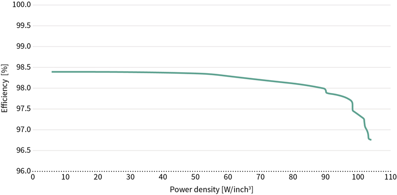
Figure 7 shows the optimization results, which indicate that efficiencies close to 98.5 percent can be achieved for medium power densities (around 40 W/in3). Alternatively, from the oppositive perspective, designs with more than 80W/in3 can be achieved at efficiencies of 98 percent.
Click image to enlarge
Figure 7: Optimization results of the entire 48V server power supply showing efficiency versus density for a system comprising a SiC-based PFC stage and an all-GaN LLC stage
In a nutshell
The application studies performed show an exact value for wide-bandgap semiconductors in server power supply designs, allowing to push both efficiency and density frontiers.
In this article, Infineon showed why SiC and GaN are the technology of choice for cutting-edge server power supplies, offering essential performance benefits in terms of efficiency and power density compared to the next best Si alternative.
The design of a complete server power supply system demonstrated a path towards either 98.5 percent efficiency or a density of more than 80 W/in³ for 48 V servers, resulting in significant OPEX and CAPEX savings.
At the same time, we show how Infineon’s CoolSiC™ and CoolGaN™ respective technologies allow us to use more straightforward control schemes, such as CCM modulation in the PFC stage, due to its hard switching capabilities. Furthermore, the performance benefit of MV GaN components for synchronous rectification in the LLC stage has been shown.
To find out more about Infineon’s designated highly-efficient wide-bandgap technologies and its full system product portfolio of switches and drivers, please visit our WBG website.
[1] More details on MV CoolGaN™ products will be available soon


