Li-Ion cells can be dangerous if not managed properly, so a battery management system (BMS) is used to ensure safe operation
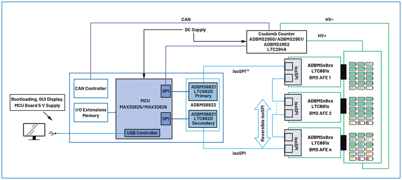
Figure 1: A simplified BMS block diagram supported with ADI BMS solutions
If Li-Ion cells are overcharged, they can undergo thermal runaway and explode. If overly discharged, chemical reactions take place within the cell that permanently affect its ability to hold charge. Both cases involve the loss of battery cells in dangerous and expensive ways.
Additionally, BMS are needed since Li-Ion cells are often stacked together to form a battery pack. Charging of stacked cells is often done in series by applying a constant current source in parallel with the stack. However, this brings with it the challenge of balancing, which is the act of keeping all cells at the same state of charge (SOC). How can we charge or discharge all cells fully without overcharging or over discharging anyone individual cell in the battery stack? Balancing is one of the many critical benefits of a good BMS. The BMS’s primary functions include, monitoring cell parameters such as cell voltage, cell temperature, and the current flowing in and out of the cell; calculating the SOC by measuring the above-mentioned parameters as well as the charge and discharge current in ampere-second (As) using a coulomb counter; and passive cell balancing to ensure that all cells are at the same SOC.
Battery Management System Solutions
Analog Devices’ ADBMSxxxx family of BMS devices use a microcontroller to communicate with the BMS, receiving the measurement data and performing computations to determine the SOC and other parameters. While most microcontrollers can communicate with a BMS, not all are suitable. A microcontroller with extensive processing power is desirable. The data that the BMS feeds back can be large, particularly when a large cell stack is required (some stacks can reach 1500 V and are composed of up to 32 ADBMS1818s connected in a daisy chain). In this case, the microcontroller must have large enough bandwidth to communicate with the different BMS ICs in the system while processing the results. As part of the BMS platform solution, the MAX32626 microcontroller has two supply sources that are managed through a PowerPath controller. The PowerPath controller prioritizes the supply source based on board power demand (connected peripherals and processing load, etc.).
Most ADI monitoring ICs come in a stackable architecture for high voltage systems, which means that multiple analog front ends (AFEs) can be connected in a daisy chain. Therefore, one of the main characteristics of the BMS controller board, referred to as the energy storage controller unit (ESCU), is that it works with multiple AFEs at the same time.
Figure 1 illustrates a typical BMS block diagram where the ESCU is highlighted inblue. While the ESCU is not optimized for functional safety applications, the user can implement protection circuits and/or redundancies to achieve certain Safety Integrity Level (SIL) requirements.
BMS Controller Board Hardware and Software
ADI’s ESCU interfaces with a variety of BMS devices (AFE, gas gauge, isoSPI transceiver). The highlights of the BMS controller board’s hardware and components are:
► On-board MCU: The Arm Cortex-M4 MAX32626 is suitable for energy storage applications. It operates at low power and has an internal oscillator running at frequencies up to 96 MHz. In low power mode, it can run at speeds as low as 4 MHz. It has excellent power management features such as a 600 nA low power mode current and an enabled real-time clock (RTC). The MAX32626 also hosts an optimal variety of peripherals including SPI, UART, I2C, 1-Wire interface, USB 2.0, PWM engines, 10-bit ADC, and many others. A trust protection unit (TPU) with advanced security features is incorporated in this MCU.
► Interfaces:The ESCU hosts multiple interfaces:
■ SPI, I2C, and CAN.
■ isoSPI for robust and safe information transfer across a high voltage barrier.
■ USB-C to power the board and flash the MCU.
■ JTAG for microcontroller programming and debugging.
■ Arduino connector (enables more flexibility for adding Arduino-compatible boards such as an Ethernet shield, sensor boards, or even a Proto Shield).
► isoSPI transceivers: Contains 2× LTC6820 to achieve the isoSPI communication with the BMS ICs on a daisy chain using a single transformer. This ensures that this board is fully isolated from the BMS ICs connected to large voltage battery stacks. The presence of a dual isoSPI transceiver provides a redundant and reversible isolated communication where the host MCU alternates communication ports to monitor signal integrity (a future development of this board will include the ADBMS6822 (dual isoSPI transceiver) for higher data rates and support of the low power cell monitoring (LPCM) function that is present in the latest ADI BMS ICs).
► Power management:
■ Power can be supplied by either a DC jack or a USB connected to the PC via a USB 2.0 interface (a USB-C connector is available).
■ A prioritizer circuit, using the LTC4415, manages and selects the supply source. It chooses between the DC jack or USB-C input based on the load at the controller and peripherals’ side. For example, if an Arduino shield is connected and running, the power consumption of the board will increase beyond what USB-C can provide. The ideal diode-OR architecture of the LTC4415 will then switch over to select the DC jack as a supply source.
■ The power chain provides different voltage rails (3.3V, 2.5V, and 5V), which are configurable through jumpers.
► Safety and protection: The MAX32626 controls an on-board isolated gatedriver, ADuM4120, that drives an N-FET connected to an external contactor (which sits on the battery board, for example). This has a protection function as the MCU will switch the MOSFET on and off through the ADuM4120 to open the contactors and disconnect the batteries in emergency or fault cases.
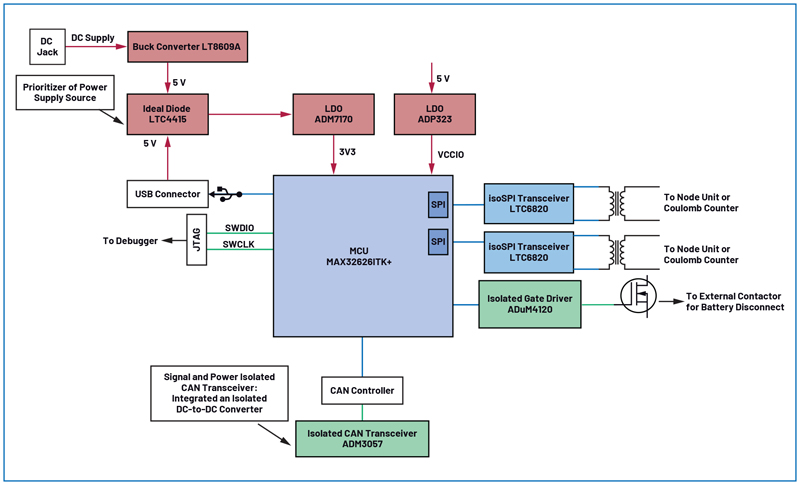
Figure 2 illustrates a high-level block diagram highlighting the main elements of the ESCU.
Click image to enlarge
Figure 2: A detailed hardware block diagram of the ESCU
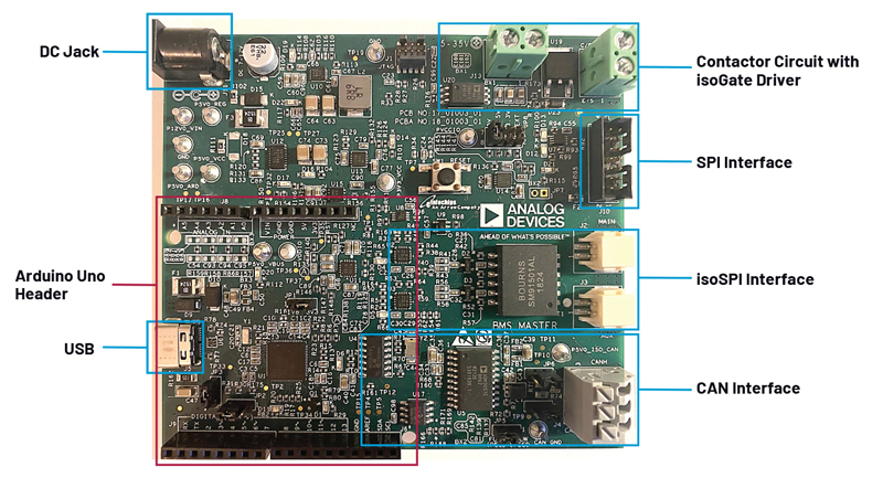
The PCB comes in a small factor of 10cm × 9cm. The main interfaces are shown in Figure 3.
Click image to enlarge
Figure 3: The top side of the ESCU
Software Information
On the software side, ADI provides a complete solution that includes an open-source graphical user interface (GUI) that can be used to communicate with the controller board. The GUI supports up to three ADBMS devices connected to the daisy chain.
The GUI communicates with the MCU through a well-defined open-source communication protocol that can be easily extended. The protocol defines messages that are sent to the MCU over the serial port. The messages are cyclic redundancy check (CRC)-protected to enable error detection. These messages allow the user to connect and disconnect with the MCU in an orderly fashion; set system parameters, perform measurements, enable and check for faults, and write any necessary commands to the ADBMS part. The application code in the MCU makes use of free RTOS threads to perform parallel operations. This is useful because a measurement thread can run in parallel with a fault-checking thread so that a fault interval time can be implemented.
A software interface is provided with the BMS controller board and is written in Python. The main user sections include a System tab, which is the main landing page of the application (Figure 4). It allows the user to establish the serial PC communication, select the number of connected AFE boards, and determine the measurement interval and thresholds to be used for overvoltage and undervoltage checks. After hitting connect, the user is ready to start measurements. If both System Status lights turn green (as in Figure 4), the measurement tabs appear depending on the number of boards entered by the user.
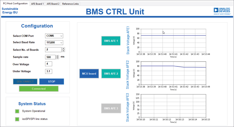
Click image to enlarge
Figure 4: System tab of user application
The BMS tab/s, illustrated in Figure 5, display the measurements processed bythe ESCU to each connected AFE. The BMS tab/s contain the cell and GPIO voltages, status, and fault readings by the AFE board. The cell voltage measurementis also graphically represented and plotted in real time.
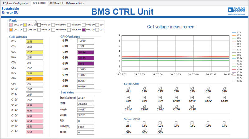
Click image to enlarge
Figure 5: BMS measurement tabs
1. The Reference tab GUI includes a reference tab representing a high level block diagram of the board and schematics. The schematics and Gerber files along with the evaluation firmware, GUI, and user guide are open-source and provided by ADI.