Of course, the latest generation technology is the best yet! But how and why?
Figure 1: On resistance x die area FoM at room temperature and 175°C
The strengths of silicon carbide fit well with the goals of automotive electrification, enabling greater energy efficiency and relieving thermal management challenges in traction inverters, on-board chargers, DC/DC converters, and mechatronic modules.
However, automotive markets always demand greater reliability and performance, with lower cost. Silicon carbide component manufacturers are responding with technical developments to increase robustness and improve figures of merit, especially at high temperature. In addition, increasing wafer sizes and foundry capacity enables the industry to satisfy automotive volume demands and realize economies of scale.
It Starts with the Crystal
As a semiconductor device substrate, silicon carbide is known to be more difficult to work with than pure silicon. From the very beginning, at crystal formation as the raw boule is grown before being ground and wafered, defects can form in the compound structure. To form perfect crystals, process parameters including pressure, temperature, stoichiometric ratio, and the rate of cooling, must be perfectly controlled. Inevitably, small deviations occur that can lead to imperfections such as vacancies, interstitial defects, and misalignments that cause dislocations and grain boundaries.
Also, SiC is renowned for its hardness so wafering is time-consuming and expensive. After wafering, followed by grinding and polishing, raw wafers can still contain defects. Subsequently applying epitaxy can compensate for some of these, although others typically remain and can affect the operating parameters and performance of devices fabricated at those sites.
Achieving surface flatness is also challenging, due to SiC’s inherent hardness. This is important to ease focusing of the lithographic equipment, which directly affects the resulting device parameters. Flatness needs to be established at individual die sites, as well as across the surface of the wafer. Both are necessary, to ensure accurate control of the parameters and to minimize parameter spread between different devices produced from the same wafer.
In subsequent processing of the wafer, defects can affect the epitaxy that adds pure and perfect crystalline layers, aligned with the wafer’s crystal structure, to create the foundation on which SiC components can be fabricated. The epitaxy may cover smaller wafer defects and prevent them affecting device performance. However, other defects can cause phenomena such as irregular step formations, dislocations, and inconsistencies above and below the epi surface.
Device Development
Clearly, improvements in crystal growth and wafering processes enable the production of epiwafers that display uniform high quality, as the starting point for high-yield component fabrication meeting market expectations for performance, reliability, and cost.
For component manufacturers, developing the epitaxy and doping processes provide the main opportunities for improving the device characteristics to meet the demands of target markets such as automotive. These are the key areas where STMicroelectronics focused its attention when creating the fourth generation of its SiC portfolio, which was made available for lead customers in 2024.
ST’s vertically integrated SiC manufacturing strategy let the engineering team optimize the wafer epitaxy to increase resilience against single-event effects and unavoidable cumulative component damage that can cause leakage currents. Evolving the epitaxy also allowed fine-tuning the behavior of the SiC MOSFET’s intrinsic body diode for faster, more energy-efficient turn-on with reduced electromagnetic emission.
Another focus of ST’s fourth-generation SiC technology development was to optimize the doping process, seeking to improve the MOSFET on-resistance and hence permit lower system power dissipation. In addition to the difficulties experienced in SiC wafer production and epitaxy, already discussed, doping SiC substrates is also more challenging than with silicon. SiC has relatively low solubility for dopant atoms, making high concentrations and sharply defined device junctions difficult to achieve. Also, the dopant activation energy is higher in SiC. Moreover, SiC’s hardness resists conventional doping by ion implantation, and so may cause damage to the crystal structure. High-temperature annealing can repair the damage as well as activate dopants, at the cost of extra complexity in component production.
Overcoming these issues achieved a further 15% improvement in the MOSFET on-resistance x active-area figure of merit (FoM), compared to the previous (3rd)-generation SiC technology. It’s worth noting that the third generation was 30% better than the second, which shows how SiC technology is continuing to make rapid advances. Ultimately, these improvements drastically reduce power dissipation in systems like the traction inverters of EVs. In fact, the fourth-generation devices are conceived predominantly for automotive traction inverter applications, with best-in-class FoM at high temperatures (figure 1) and extended robustness under real traction inverter stress conditions.
Improved Protection
ST’s fourth-generation SiC technology development team also designed enhanced edge terminations, which are structures integrated in the substrate to increase ruggedness and reliability. These are typically positioned at the periphery of power semiconductors to protect against the effects of excessive electric field strength caused by uneven concentrations of field around junctions or other features at the device edges. The field strength can exceed the device breakdown voltage locally, resulting in early failure. Edge protection therefore has a critical impact on robustness and reliability and is typically implemented with structures such as field guard rings (FGR), junction termination extensions (JTE), or combinations of these. However, edge termination can occupy a large area so improvements must be space efficient to prevent packaged devices having excessively large footprint.
Improving the edge termination calls for a structure that provides effective protection up to the desired breakdown voltage within the smallest possible area to ensure the overall efficiency of the device. Designing an effective and compact termination is complicated because SiC is such a challenging material to work with. In addition to slow and difficult diffusion of dopants, the selection of suitable dielectric materials is limited.
The patented edge termination of ST’s fourth-generation SiC technology is proven to manage the electric field distribution and is customized to handle the most challenging automotive mission profile.
In addition to improving process controls to drive out the causes of defects in wafers and epitaxy, effectively raising quality, the device yield per wafer can also be improved by increasing quantity. Early commercial SiC devices were produced on small-diameter wafers, one wafer at a time. With growing commercial maturity, typical production processes have progressed to larger reactors capable of handling multiple wafers simultaneously, with consistent wafer-to-wafer quality. In addition, larger wafer sizes position component manufacturers to respond to high component volumes demanded for markets such as automotive as well as the emerging green energy segment.
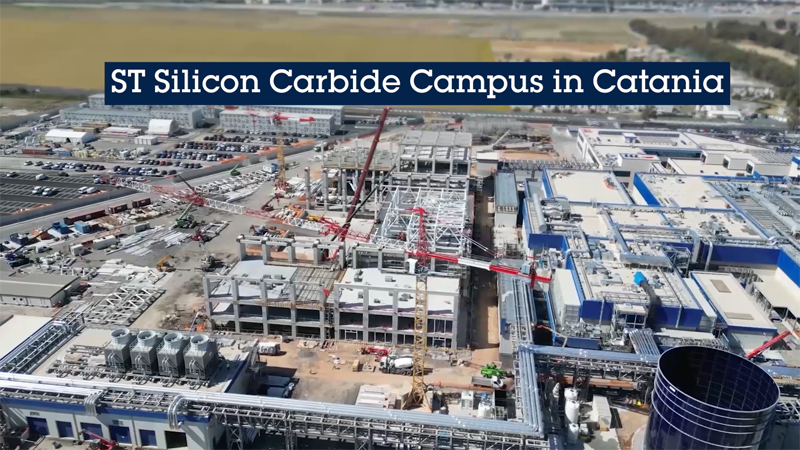
To increase production volume and supply-chain resilience, ST qualified its 200mm wafer fabrication facility in 2023 and has announced a multi-billion-dollar investment program at its SiC campus in Catania, Sicily. This will create the world’s first fully integrated silicon carbide facility (figure 2). Production is scheduled to start in 2026. Also, in a joint venture with Chinese manufacturer Sanan, ST will begin SiC device manufacture in Chongqing, China, in Q4 2025.
Click image to enlarge
Figure 2: The world’s first fully integrated silicon carbide facility, in Catania
Conclusion
The improvements achieved with each successive generation of SiC technology deliver new components that result in greater efficiency, reliability, and robustness. Combined with investment in capacity to produce larger volumes, devices can be deployed more effectively in the automotive industry, throughout a wider variety of vehicle platforms aimed at different market segments. The same advancements also make higher-performing, longer-lasting, and more economical parts available for markets such as industrial, renewable energy generation and storage and power supply for AI server.


