Author:
Victor Khasiev, Analog Devices, Inc.
Date
06/12/2024
 PDF
PDF

Click image to enlarge
Figure 1: Electrical schematic of LT8711 for SEPIC and buck applications.
The LT8711is a dc-to-dc controller that supports synchronous buck, boost, single-ended primary-inductor converter (SEPIC), and ZETAtopologies, or nonsynchronous buck-boost topologies. Analog Devices offers numerous synchronous buck and boost converters and regulators, but the synchronous SEPIC topology is somewhat rare. Nevertheless, the SEPIC topology is useful because it supports a stable output voltage level even as the input voltage drops far below the output or rises far above it. This feature can be indispensable in automotive electronics, especially during cold cranking and load dumps, and in industrial applications due to long supply lines and brownouts in factory settings. Oil and gas devices can increase reliability by using SEPIC converters to supply critical loads from multiple and varied power supplies and, if one supply fails, the SEPIC can use another supply to support the load, even if the input is at a different voltage level.
Circuit Description and Functionality
Figure 1 shows the schematic for a synchronous SEPIC converter using the LT8711, which controls a power train consisting of:
► Two noncoupled inductors, L1 and L2
► Modulating N-channel MOSFET, MN1, driven from pin BG
► Two synchronous P-channel MOSFETs, MP1 and MP2, driven from pin TG
► Decoupling capacitors, C1, C2, and C3
► Input and output filters
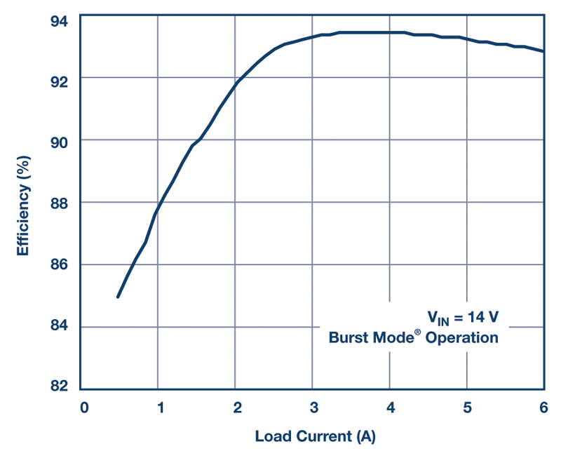
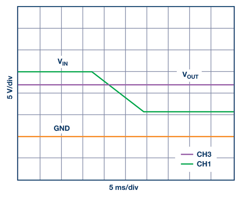
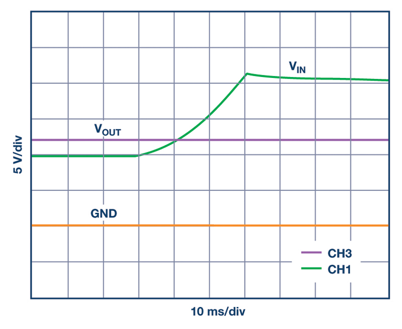
Figure 2 shows the efficiency of the converter with a 14 V input voltage. The synchronous scheme keeps efficiency high, reaching 93.4% at the peak. Figures 3 and 4 show output regulation as the input voltage falls below, and rises above, the output, which remains stable.
The standard demo circuit DC2493A was reworked to increase output current from 4 A to 6 A. The MOSFETs MN1 and MP1, and inductor L2 were replaced by the components shown in Figure 1.
Click image to enlarge
Figure 2: Efficiency of the LT8711 SEPIC.
Click image to enlarge
Figure 3: Model of a cold cranking event. The rail voltage VIN drops from 15 V to 6 V, but VOUT remains stable at 12 V.
Click image to enlarge
Figure 4: Model of a load dump. The rail voltage rises from 10 V to 20 V, but Vout stays in regulation.
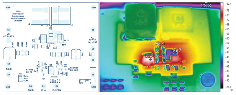
A modified demonstration circuit, DC2493A, was used to evaluate this design. The thermal image of the modified board is shown in Figure 5. The LTspice® model of a similar solution can be found inthe LT8711 demo circuit. The detailed recommendation for the selection SEPIC power train components can be found in the LT8711 data sheet.
Below are basic expressions of peak voltages and currents for understanding the functionality of this topology.
IL1= IIN+ ΔIL1
IL2 = IOUT + ΔIL2
VBG= VTG= VIN + VOUT
ITG= IBG= IIN + IOUT+ ΔI/2
Click image to enlarge
Figure 5: A DC2493A and a thermal map of the operating SEPIC (VIN 14 V, VOUT 12 V at 6 A). The hottest component is MNI at 77°C.
Conclusion
The LT8711 is a versatile and flexible controller designed for use in synchronous buck, boost, SEPIC, ZETA, and nonsynchronous buck-boost converters. In particular, the synchronous SEPIC can be used to produce efficient outputs that fall somewhere in the middle of the input voltage range, which is particularly important for automotive and industrial applications.