This article discusses the merits of a new control IC specifically designed to improve on the performance of a high side buck controller. Tighter current regulation may result in savings as fewer LEDs may be required to guarantee a certain lighting level, not a small consideration in cost sensitive applications. Other benefits of this new control IC are highlighted as well. The high side buck converter topology is a universal topology for driving high brightness LEDs, that is finding its way into just about any application in low- and high-end markets. The high side buck converter topology is not much different from the standard buck converter topology, with the difference being that the power stage components are rearranged, so that the MOSFET is attached to the low side and the LED string and catch diode are attached to the high side. Doing this removes the need for level shifting of the gate signal, thereby lowering the cost of the gate driving circuit.
In general, we desire accurate control over the average value of the LED current. The typical high side buck driver implements a peak current control scheme, being economical and simple to apply. In exchange for simplicity and low cost, initial accuracy of the average current may suffer and line and load regulation are significant. The basic design procedure is to determine the peak current threshold of the inductor current, which is based on the target value of the average LED current and the superimposed current ripple, typically 20 to 30% of average. Tolerance of parts, such as the inductor, the oscillator, comparator offset and propagation delay all affect the accuracy of the LED current, and may easily lead to errors in the 5 to 10% range. Regulation of average LED current is further affected by line and load voltage changes, which are not compensated for in a simple peak current control scheme. The lack of current regulation accuracy may lead to overdesign in the LED string or to additional circuit measures such as trimming for accuracy, line voltage or load voltage feed forward compensation, or possibly a secondary current control loop. Either way, the lack in accuracy comes back as an increase in cost or complexity. Supertex's HV9961 improves on this situation by employing a novel and proprietary average current mode control scheme that virtually eliminates errors that occur from changes in line voltage, load voltage, oscillator period, inductor value and other sources of inaccuracy while maintaining the simplicity of the peak current mode controller. With the HV9961, the average current can be maintained within 3% across line and load despite loose tolerance on the inductor, opening the possibility to lowering system cost.
The difference between the peak and the average current is commonly known as the peak to average error. This error tends to zero if ripple is very small. In practice, small ripple is impractical as it calls for a large inductor. Also, a certain amount of ripple is desirable for stable operation of the peak mode controller; if the ripple is small, then the comparator trip point becomes sensitive to noise. It is straightforward during the design stage to take the peak to average error into account by calculating the ripple from the equation below and raising the peak current threshold accordingly:

With the above equation in hand we can point to the first sources that will lead to an error in the average LED current. The true inductor ripple is affected by changes in the right hand side values of the above equation. For instance, an output voltage change brings about a like change in ripple amplitude, causing a change in the average LED current. The change is known as load regulation and can be quite substantial depending on the contemplated load voltage range. Next is ripple current change brought about by tolerance in the programmed OFF time (TOFF). For example, a 10% tolerance in TOFF in results in a like tolerance in the ripple. If ripple is 20% of the average LED current, then a 10% change in the ripple leads to a 2% change in the average LED current. Tolerance in the inductance, often in the 10% range, leads to change in the average LED current in a similar manner.
Another source of error is the peak current comparator. Offset voltage has a direct effect on the peak current amplitude and thereby on the average LED current. Although the offset voltage of some high side buck controllers can be as low as � 25mV for a temperature range of ? 40°C to + 85°C, it contributes as much as � 10% variation in the LED current even when exploiting the maximum CS threshold voltage of 250mV typical. Another cause is propagation delay, see figure.
The figure clearly shows how the inductor current runs to a larger peak value due to the current sense comparator delay ?tCS, thereby raising the average LED current. Propagation delay is also responsible for line regulation. Should the line voltage go up, then the slope of the inductor current becomes steeper, and the run up becomes larger, thereby raising the average LED current even more.
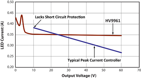
The HV9961 overcomes the above drawbacks by means of using Supertex's average mode constant current control method. The IC regulates the average inductor current directly and accurately within � 3% over a duty cycle range of 10 to 75%. A graph comparing load regulation against a typical peak current controller is shown below. The pickup in output current between 0 and 10V shows the short circuit protection of the HV9961 in action, a region where most other peak controller will experience runaway current due to minimum ON time limitations. The HV9961 also features an auto-zero circuit for the current sense input, which cancels offset and propagation delay errors.

The HV9961 performs linear dimming for a voltage at the LD pin in the range of 0 to 1.5V unlike other controllers, where the range is 0 to 250mV. Furthermore, the HV9961 produces zero current when VLD = 0V unlike many other controllers. The IC overcomes the typical limitation by disabling the Gate drive when the LD pin voltage drops below 150mV. Switching resumes when the voltage rises above 200mV. The HV9961 allows very wide range dimming by mixing PWM and linear dimming using a single square wave control signal with variable duty and amplitude.
As is typical of most converter ICs, the duty cycle, or better yet, ON time can not be arbitrarily small. Minimum ON time is determined by the need for leading edge blanking and the presence of comparator propagation delay. Minimum ON time of typical controllers is in the order of 500ns (max), and in the HV9961 it is 1?s (max). Minimum ON time can give disastrous results when a short circuit is present at the output. Under this circumstance, the inductor current will ratchet up with each passing switching cycle as the voltage responsible for bringing down the load current has been reduced to no more than the forward voltage of the catch diode. Other controllers will allow the current to staircase to a potentially damaging level.
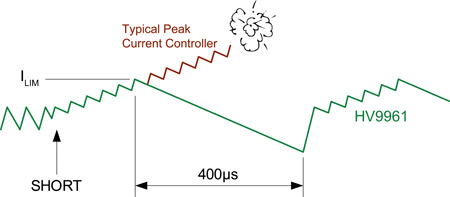
The HV9961, on the other hand, protects the LED driver by introducing an overcurrent comparator. When the threshold is reached (440mV), the GATE output is disabled for a period of 400?s, thereby letting the inductor ramp down to a safe level.
The higher current regulation accuracy of the HV9961 makes it the preferred part in most LED driving cases and gives more accurate and more uniform performance. Output short circuit protection and wide range dimming give an additional advantage to this part. www.supertex.com

