Author:
Dr. Mario Ursino, Staff System Innovation Engineer, 48 V Innovation Labs, and Dr. Roberto Rizzolatti, Senior Staff System Innovation Engineer, 48 V Innovation Labs, both at Infineon Technologies
Date
06/30/2023
 PDF
PDF

Click image to enlarge
Figure 1. Data center power architectures. Unregulated IBC for high-density applications, such as AI, accelerator cards (left), and 12-V regulated common rail (right)
Data centers consume vast volumes of power, meaning even the most minor improvements in their performance efficiency translate into significant power savings.
This article explores two novel power conversion topologies from Infineon - the Dual-stage Regulated Hybrid Switched Capacitor (DR-HSC) converter and the Regulated Hybrid Switched Capacitor (RHSC) converter, which combines a Hybrid Switched Capacitor (HSC) with a regulated stage. It discusses challenges in the design of regulated intermediate bus converters when addressing the 48 V to 12 V regulated conversion. Finally, it shows how Infineon’s OptiMOS™ Source-Down MOSFETs enable increased power conversion efficiency and density in these 48 V step-down topologies.
Power conversion architectures for data centers
The two most common 48 V data center power architectures are illustrated in Figure 1.
The first approach optimizes efficiency for a digital load (GPU/CPU) using an unregulated Intermediate Bus Converter (IBC), with regulation performed at the second stage by a Voltage Regulation Module (VRM). This configuration is mainly used for AI and accelerator cards, where power density is paramount.
The second approach uses a regulated IBC to convert 48 V to 12 V, which is always required by multiple peripherals on the server board at the rack level. The novel IBC topologies presented in this article are intended for this architecture, aiming to provide a regulated 12 V rail without compromising efficiency or power density.
DR-HSC: reducing switching frequency and output inductor dimension in a regulated converter
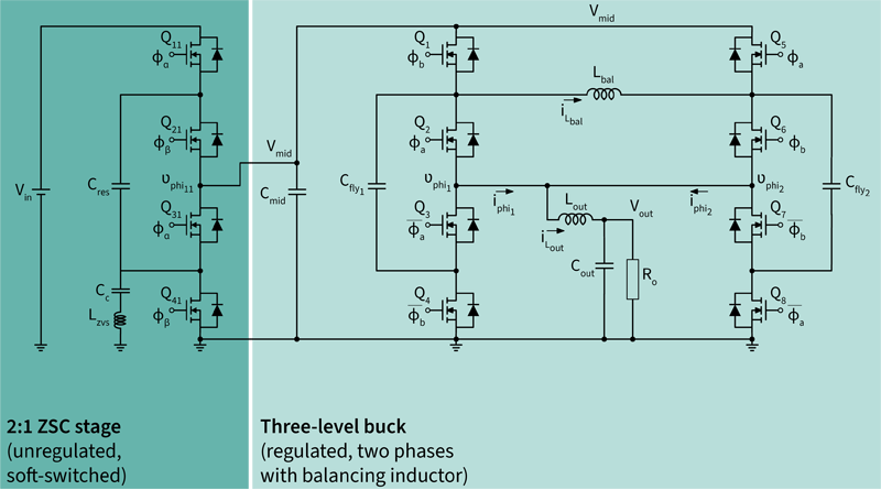
Improving power density in a converter that processes energy through an output inductor requires decreasing its magnetic flux. Infineon’s DR-HSC converter (Figure 2) enables inductor size reduction by using a cascaded switched capacitor architecture, enabling switching frequency reduction and the selection of a low-profile and low-DCR inductor. This is achieved by exciting the output inductor with a scaled version of the input voltage.
Click image to enlarge
Figure 2. Infineon’s 48 V to 12 V DR-HSC two-stage regulated converter
The first stage of the DR-HSC converter is based on a zero-voltage switched (ZVS) capacitor converter solution. This operates in a resonant mode where a series resonant tank is formed by a flying capacitor and the parasitic inductance of the MOSFET and the PCB, enabling zero voltage switching.
The ZVS inductor LZVS is used to achieve zero-voltage switching, together with a DC-blocking capacitor placed in series. The first stage efficiently reduces and divides the input voltage in half. In the second stage, a dual-phase three-level buck converter achieves high efficiency and power density in the high current domain and passive capacitor balancing through the small inductor Lbal.
As a dual-phase buck converter, it can use two pulse width modulation (PWM) signals for the multilevel bridges, each phase-shifted by 180°, resulting in four PWM signals: two for the equivalent high side and two for the low side. The size of the additional balancing inductor depends on the output voltage and the frequency of the converter.
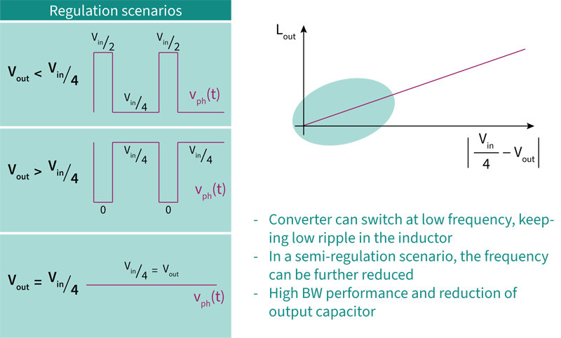
This is a three-level flying capacitor converter, so the output current ripple is twice the switching frequency; nonetheless, the converter has a nearly zero current ripple at 48 V. When the input varies, as shown in Figure 3, the three-level buck drives the output inductor with pulses at Vmid, Vmid/2 or ground. The two-phase/single-inductor operation enforces capacitor balancing on the second stage: in each switching cycle, Cfly1 and Cfly2 are connected in series, so their summed voltage must be Vmid, while the balancing inductor ensures that their voltages are also equal to Vmid/2.
Click image to enlarge
Figure 3. Reducing switching frequency and output inductance in 48 V to 12 V regulated converters
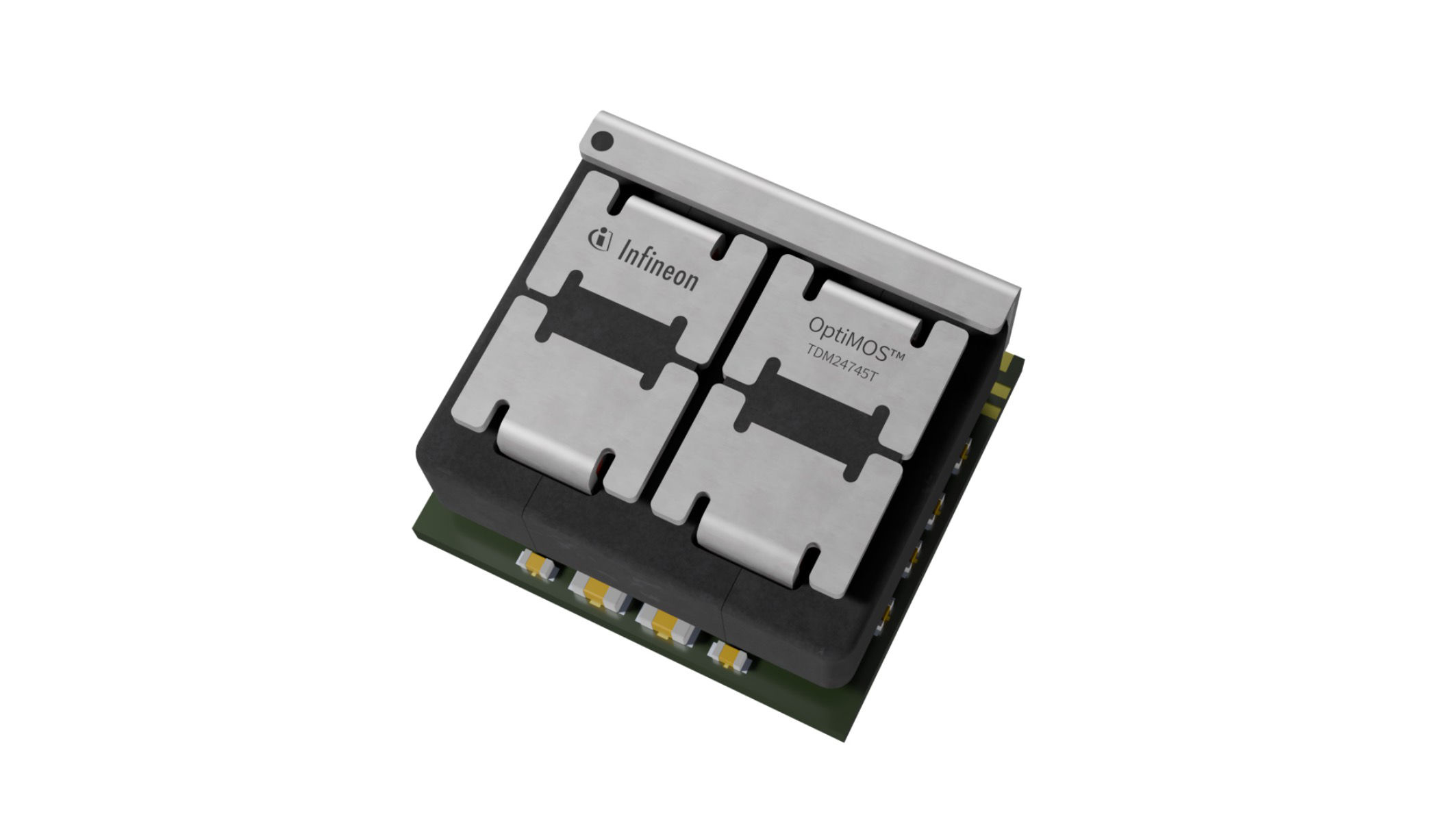
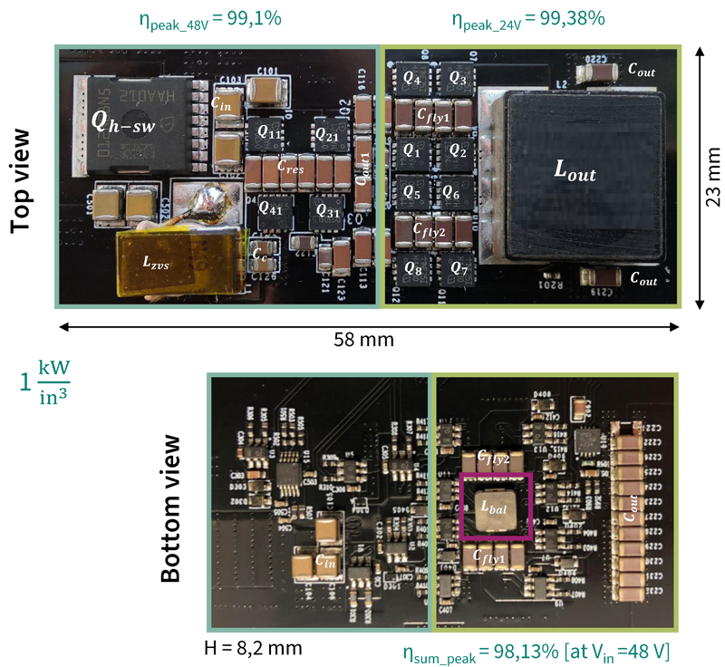
The 600 W prototype board of Figure 4 demonstrates the effectiveness of this solution: the first and second stages each have a peak efficiency above 99 percent, resulting in an overall peak efficiency of approximately 98 percent and achieving a power density of 1 kW per cubic inch. The balancing inductor is located between the two flying capacitors, so this board design is easy to implement. High efficiency in the first stage is enabled by using Infineon’s OptiMOS™ power MOSFETs 40 V Source-Down and OptiMOS™ power MOSFETs 25 V Drain-Down for the second stage. Both stages are controlled using Infineon’s XDP™ XDPP1100 digital controller in a 4 mm x 4 mm package with PMBus capability.
Click image to enlarge
Figure 4. The 600 W 48 V to 12 V DR-HSC prototype board from Infineon
RHSC: semi-regulation enabling extreme power density for the 48 V to 12 V
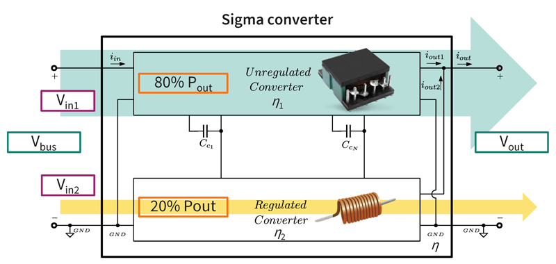
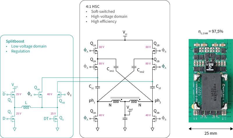
Infineon’s 4:1 RHSC-regulated converter combines the high power density of an autotransformer with the regulation capability of a boost converter. These topologies are often called Sigma (commonly used to express a summation) or ISOP (Input-Series, Output-Parallel). In fact, the input current of these blocks is the same, while the outputs are shorted.
As shown in Figure 5, the input voltage is split in favor of the unregulated converter so that 80 percent of the processed power flows through a high-efficiency and high-density path. Only 20 percent of the power is used to regulate 12 V.
Click image to enlarge
Figure 5. Infineon’s 48 V to 12 V RHSC-regulated converter
As a result, the total converter efficiency is a weighted mean of the input voltages, therefore dominated by the high-efficiency block. Differently from the classical Sigma converter, the Sigma capacitors Cs1 and Cs2 enforce the input-series behavior, as shown in Figure 6.
Click image to enlarge
Figure 6. Infineon’s RHSC 48 V to 12 V topology overview
Most power flows from 48 V to 12 V through the 4:1 resonant and unregulated block called HSC. MOSFETs in the low-voltage domain (left-hand side) operate in hard switching, while the higher-voltage domain (right-hand side) features resonant currents and zero voltage switching.
Resonance occurs between the capacitors and the leakage inductance of the autotransformer, implemented with full interleaving thanks to the lack of functional isolation need. This topology delivers high efficiency and power density – for example, temperatures at 1 kW do not exceed 60°C with fan cooling. In addition, 80 percent of power flows through the autotransformer, and since HSC power MOSFETs are soft-switched, they don’t suffer from switching losses. This also means that Infineon best-in-class Source-Down MOSFETs can be used.
The equivalent voltage supply of the boost block ranges from ground to 12 V. This converter provides full 12 V regulation between Vin = 48 V to 60 V, becoming a fixed-ratio 4:1 below 48 V. It provides 97.5 to 98 percent full load efficiency up to 1.2 kW (1.6 kW peak), achieving a high power density of 1.2 kW per cubic inch.
Summary
Infineon’s DR-HSC and RHSC converters are the right choice when a regulated 12 V rail is needed in a 48 V Data Center. DR-HSC offers layout flexibility and a low profile. On the other hand, the RHSC topology exploits the power delivery of the output autotransformer, meaning board size can be reduced through vertical size utilization, thus shrinking the overall solution footprint. In addition, this topology can replace existing fixed-ratio IBCs with comparable density and efficiency. Both topologies can achieve high efficiency and power density in regulated IBCs for 48 V to 12 V data center applications, and Infineon’s XDP™ XDPP1100 controller can fully handle both.