Author:
Yingying Wang, NXP Semiconductor,s Nijmegen, The Netherlands
Date
01/19/2011
The current market of Switch Mode Power Supply IC's shows increasing demand on efficient and cost effective solutions that enable slim and compact design. The industry standard Energy Star Version 2.0 requires the external power supplies to have average active mode efficiency higher than 87% and no load standby power lower than 300mW (output power <50W), or 500mW (output power from 50W to 250W). Many customers actually have even more demanding requirements such as standby power less than 100mW. With the GreenChip TEA1733 flyback controller, 90% efficiency and less than 100mW standby power can be simultaneously obtained with minimum amount of external components. A 65W/19.5V demo board for notebook adapter is shown in Figure 1. The TEA1733 is suitable for almost all applications with power requirement up to 75W. Typical applications include netbook adapters, LCD monitors and printer adapters. This controller can be used in Discontinuous Conduction Mode (DCM) as well as Continuous Conduction Mode (CCM). The combination of fixed frequency operation at high output power and frequency reduction at low output power provides high efficiency over the total load range. Frequency jitter is implemented to reduce electromagnetic interference (EMI). The IC is also equipped with several protections to enhance robustness and reliability.

Fixed frequency flyback converter A flyback converter is the most ubiquitous switched mode power supply topology today. The typical configuration of the TEA1733 in a flyback topology is shown in Figure 2. The TEA1733 uses peak current control and the output power is regulated by the CTRL pin. The load is measured and transferred back to the CTRL pin via an optocoupler. The primary current across an external resistor R1 is sensed through the ISENSE pin. Its peak is compared and adjusted with an internal voltage, which is proportional to the CTRL voltage. By controlling the peak current, the duty cycle is adjusted accordingly. When the duty cycle is above 50%, slope compensation is activated to avoid sub-harmonic distortion. The maximum duty cycle is limited at 74%. In low power operation the switching losses are reduced by lowering the switching frequency. An internal Voltage Controlled Oscillator (VCO) reduces the frequency gradually down to 0Hz. To prevent audible noise, the peak current is set to 25% of the maximum peak current as the frequency reduces. The frequency and peak current control curves can be found in Figure 3.

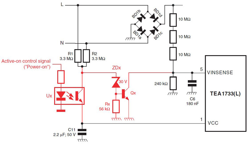
The TEA1733 integrates frequency jitter in order to reduce EMI emission. The center frequency of 66.5kHz is smeared over +/- 4kHz by a jitter oscillator. The frequency of the jitter oscillator is chosen to be 260Hz to avoid the audible noise. During start-up, the supply voltage VCC is charged by the current through a start-up resistor, and the current consumption of the IC is only around 10μA. No high voltage start-up circuit is required. As soon as VCC reaches its start-up level of about 20.6V, and all the other conditions are met, the controller starts to switch. From that moment on, the supply voltage is taken over by the auxiliary winding of the transformer. The normal operating current is typically 0.5mA excluding load at the DRIVER pin. The low current consumption helps to increase the efficiency. Standby operation Because of the low current consumption and frequency reduction, a standby power of less than 100mW can be achieved by using TEA1733. With proper choice of external components such as resistors and the X-cap, the measured standby power is 48mW at 115VAC and 84mW at 230VAC for a typical 65W, 19.5V power supply. If there is an external "Power on/down" signal available to indicate the standby mode, like the battery operated equipment, the standby power can be further reduced to below 30mW by switching off the entire application. This is referred to as "Zero Watt" design. The basic application diagram of "active off" situation is shown in Figure 4, in which the external "Power-down" signal turns high during the standby mode. Then Transistor Qx conducts and pulls down the VINSENSE voltage, which initiates the restart protection. The IC immediately stops switching and enters power-down mode. In the power-down mode, the IC consumes only 10μA current. In the meantime, VCC is clamped to just below the start-up level to guarantee a quick restart after a standby situation.

Protections TEA1733 features various protections, for instance, Input Over-Voltage/Under-Voltage Protection, Output Over-Voltage Protection, Over-Power Protection, and internal/external Over-Temperature Protection. The above protections lead to either safe restart or latched protection. For safe restart protection, the IC goes into power-down mode first, and wakes up when all the conditions are satisfied. In the power-down mode the OPTIMER pin is quickly charged to 4.5V and then slowly discharged to 1.2V. In a latched protection, the IC also goes into power-down mode, but the VCC voltage is clamped to around 6V. In order to reset the latched protection, the VCC voltage has to go below a certain level by unplugging the mains. The 6V clamp is just above that level to enables fast reset after a latched protection. A special function of TEA1733 is that the PROTECT pin can realize two protections: external Over-Temperature Protection and Output Over-Voltage Protection, as illustrated in Figure 5. The PROTECT pin has the current source capability of 32μA and sink capability of 107μA. The internal circuit tries to regulate the PROTECT pin to 0.68V. No protection will be set if the PROTECT voltage is between 0.5V to 0.8V. If the VCC is so high that the maximum sink current is not able to pull the PROTECT voltage below 0.8V, Output Over-Voltage is detected. This protection can be used with general purpose. With increasing temperature, the resistance of the negative temperature coefficient (NTC) thermistor connected at the PROTECT pin decreases. If the maximum source current is insufficient to keep the PROTECT voltage above 0.5V, external Over-Temperature is detected. Both situations lead to the latched protection.

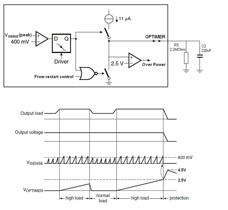
Adjustable over power time-out Temporary over load situation is allowed if the OPTIMER pin is connected as Figure 6. When ISENSE peak voltage is above 400mV, 11?A current flows out of the OPTIMER pin to charge the external capacitor C2 and the over power timer starts. For long over load situation, the Over-Power Protection is activated as soon as the OPTIEMR voltage exceeds 2.5V. For short over load situation, if the ISENSE peak voltage drops below 400mV before the OPTIMER voltage reaches 2.5V, C2 will be immediately discharged and no protection will happen. The over power time can be adjusted by choosing different values of C2 and R3.

High/low line compensation In fixed frequency CCM the maximum output power depends not only on the primary peak current but also on the duty cycle and therefore the input voltage. The TEA1733 has built-in input voltage compensation to ensure accurate Over-Power Protection that is nearly constant over the full mains. The over-power compensation circuit measures the mains voltage via the VINSENSE pin, and converts it to a current flowing out of the ISENSE pin. This current generates a voltage across the soft start resistor R2 in Figure 2, which limits the maximum current through the sense resistor R1. By proper tuning of R2, the maximum output power becomes independent of the input voltage. Available versions The TEA1733 has several versions to meet the requirement of different applications. The standard version causes safe restart for over power time-out. The TEA1733L triggers latched protection for over power time-out. Derivatives operating at 90kHz are available in a safe restart version as TEA1733A and a latched protection version as TEA1733M. Besides SO8 package, the TEA1733(L) IC is also available in DIP8 package, known as TEA1733(L)P. Conclusion The TEA1733 has become the first product in the complete new GreenChip series of lower power AC-to-DC control IC's launched by NXP Semiconductors. Its high level of integration makes it possible to fulfill the growing demand on low cost and compact power supply designs. Less than 30mW standby power is achieved with "Zero Watt" design. The power performance especially at standby mode distinguishes it from other controllers for low-power computing and communication applications. www.nxp.com