Analog Devices has expanded its range of Silent Switcher devices to include a buck-boost converter for the first time.
A few months ago in this column, I talked to Frederik Dostal of Analog Devices about the Silent Switcher technology that was incorporated into the company’s range of buck converters. Recently, Analog Devices has added the LT8350S to its Silent Switcher portfolio. The significance of this product is that it boasts a buck-boost topology. I took time out to talk to Frederik to find out more about the device and how it operates.
Similarly to Analog Devices’ other Silent Switcher products, the LT8350S was developed primarily to reduce the noise generated in the voltage conversion circuit. Today’s voltage conversions employ high frequency operation to maximize efficiency and reduce solution size. There is a downside in that those high frequencies introduce noise into the circuit in the form of EMI. The company’s buck converter range is effective at cutting that EMI, but there are other types of circuits that require the input voltage to be both up-converted and down-converted when necessary. For example, battery powered applications need a converter to reduce the voltage when the battery is full, but as the battery drains, its output voltage decreases until it is below the desired output voltage of the converter and therefore needs to be boosted. This type of conversion is also needed where the power supply is irregular or when heavy loads, such as those in automotive applications, cause the battery voltage to drop. Buck-boost converters are normally the preferred method of accomplishing this type of conversion.
Buck conversion Silent Switcher devices effectively split the current into two hot loops that generate magnetic fields that are directly opposed, cancelling any noise. The buck-boost LTC8350S uses the same technique, but with four loops - two in the buck circuit and two in the boost circuit. Although this method works well, noise can occur when the device switches from buck to boost, or vice versa because the MOSFET resets and the magnetic fields collapse when the changeover is made. To combat this effect, the company has designed in two extra modes for when the converter’s input voltage is close to its output voltage, one on the boost side and one on the buck side. This provides better noise performance during transitions. The Silent Switcher devices also use SSFM (spread spectrum frequency modulation) to reduce EMI peaks at individual frequencies. Finally, the Silent Switcher devices have copper pillars instead of bonding wires between the die and the lead-frame to reduce parasitic inductance. Together, these technologies help the LT8350S to reduce all types of noise over its entire operation range of up to 2MHz without slowing down switching edges to provide efficient conversion. Additionally, the design only uses a single inductor for all conversions, proving a smaller overall solution with lower BoM.
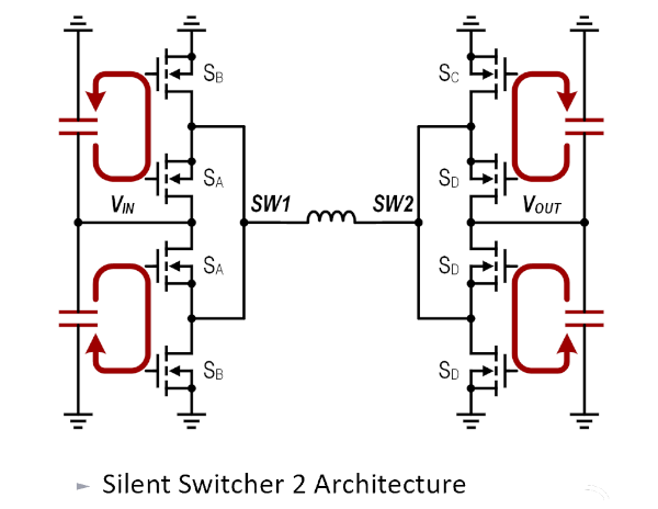
The LT8350S is designed to convert input voltages from 3V to 40V to output voltages of between 1V to 18V, up to a maximum current of 6A at efficiencies that can reach 95%. It uses Analog Devices’ second generation of Silent Switcher technology, which incorporates more components into the package, including the loop capacitors. Including these capacitors in the package reduces the trace length of the loop and allows them to be matched more precisely. An alternative version of the device is also available with exactly the same specifications, but which needs external loop capacitors. This device, the LT8350, is mainly intended for applications in extreme temperatures which go beyond the specification of the internal capacitors.