A Winning Combination of AlN Ceramic Substrate and SiC MOSFETs

In recent years, the demand for small and long-lasting power electronic designs has been rising across various markets, from electric vehicles to renewable energy systems
Figure 1: Typical thermal stack of a baseplate-less module, and RthJA distribution
Wide bandgap silicon carbide (SiC) has emerged as a crucial semiconductor, particularly in applications that demand high power density and efficiency, such as EV charging, solar inverters, or energy storage systems. Its key advantages over traditional silicon devices include higher breakthrough electric field, larger thermal conductivity, higher electron-saturation velocity, and lower intrinsic carrier concentration.
The fast-switching capability of SiC MOSFETs makes them particularly suitable for applications that operate at high frequencies. These applications range from hard-switching AC-DC stages exceeding 30 kHz to quasi-resonant or fully resonant topologies. They exhibit a significantly lower temperature dependence compared to Si IGBTs, lack a tail current during turn-off, and have lower input and output capacitances. These collectively contribute to decreased switching losses, and low switching losses (Esw) are pivotal for high switching frequencies. Thus, SiC MOSFETs allow for smaller passive components, resulting in more compact and efficient power converters.
However, the power cycling capability of SiC devices has been found to be lower than that of Si devices in the same current and voltage classes. The mechanism of aging in SiC devices is well understood. It is largely related to the degradation of the chip solder when soft soldering and aluminum bond wires are used. The unique material properties of SiC, including higher thermal conductivity, can lead to higher temperatures at the chip edge. Also, its higher Young’s modulus puts greater stress on the chip solder during power cycling.
To address the issue of chip-solder degradation, Infineon has introduced Easy1B and Easy2B modules that combine an aluminum nitride (AlN) ceramic substrate with the SiC MOSFET technology.
Use of Power Modules
Power modules, such as the Easy1B and Easy2B, offer enhanced power density and streamline the assembly process, simplifying or enabling automation. The integration of a ceramic insulator layer facilitates the isolation of high voltage from the heat sink. Through press-fit technology, these modules can be directly attached to the PCB without the need for a soldering process. A pre-applied thermal interface material eliminates the additional manual steps in the production line and allows for direct mounting onto the cooling plate.
Beyond saving time during the mounting process, press-fit pins significantly reduce both electrical and thermal contact resistance, making the technology a perfect fit for a wide range of currents. The gas-tight, vibration-resilient contact offers best-in-class reliability in different environments.
Within the Easy family, pins are soldered directly onto the direct copper bonding (DCB) substrate via rivets. This design allows for the power and control pins to be as close to the dies as possible. Thus, minimizing the commutation and control loops and optimizing performance.
The concept of modules incorporates chip parallelization, which guarantees optimal current sharing and uniform power dissipation across the product’s entire footprint. This eliminates the requirement for paralleling smaller devices at the PCB level. The considerable flexibility supports the mixing of different technologies and the realization of complex topologies in an optimal, symmetric, and low-inductive manner.
Modules without a baseplate offer a more compact and lightweight design, making them well suited for space-constrained applications where size and weight are critical considerations. This compactness provides greater flexibility in system integration and miniaturization.
Thermal Performance
Effective thermal management is essential in power electronics design as it directly influences the efficiency and reliability of the power modules. Although Easy SiC modules can run at 175°C, operating under high temperatures significantly increases the conduction losses and reduces the output current and system efficiency. It can also compromise the performance and safety of the cooling concept. To operate at higher temperatures, costlier PCB materials and components rated for higher temperatures might be required.
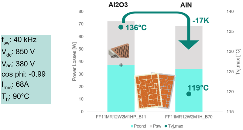
Incorporating an AlN ceramic substrate into a baseplate-less SiC power module offers numerous benefits over traditional solutions, especially related to thermal performance. AlN offers superior thermal conductivity performance, which is seven to eight times higher than that of the widely used aluminum oxide (Al2O3).
In a typical thermal stack of a baseplate-less module, the configuration begins with the die, followed by a chip-solder layer, then a layer of copper (in which the layout is done), an insulating ceramic substrate, and another layer of copper. Finally, topped with thermal grease. The assembly is usually mounted onto an external cooling mechanism, which may be forced-air cooling or water cooling. In such a setup with the well-known Al2O3, the DCB substrate significantly impacts the total junction-to-ambient thermal resistance, RthJA (Figure 1). Its contribution can exceed 50%, although the precise value will depend on several factors, including chip size, layout, and the type of thermal grease used.
All in all, using AlN ceramic substrate potentially results in up to 40% reduction in RthJA. As the used AlN substrate is thicker, the thickness of the thermal grease can potentially be reduced due to the improved cavity profile.
The choice of material for the DCB plays a crucial role in determining the overall thermal performance of the power module. A lower RthJA will lead to reduced operating temperatures under typical conditions (Figure 2), and thus, reduced temperature swings and increased lifetime.
Click image to enlarge
Figure 2: Loss and temperature simulation of an Easy2B module using Al2O3 and AlN ceramic
Power-Cycling Capability
It is, however, not just about the thermal performance. Additional thermo-mechanical simulations have shown that using an AlN substrate can:
- Improve the thermal spreading due to higher thermal conductivity. This results in a lower ceramic lateral thermal gradient, and hence lower ceramic stress during active heating.
- Reduce the accumulated plastic strain on the chip edge. This leads to lower risk of delamination at the edges between the chip solder and the top copper.
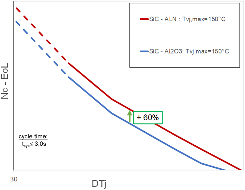
The combination of the abovementioned factors substantially enhanced the capability of the test devices during power cycling (PC) tests. The results demonstrated a remarkable improvement, with the number of cycles in power cycling stress being increased by a factor of 1.6, for the same dT, Tvj,max and ton, when compared to Al2O3 based solution (Figure 3), with no additional changes made to the design. For a temperature swing of 50 K and a peak of 125°C, the Al2O3-based solution achieved around 150000 cycles before it failed. The EoL is defined as more than 20% increase in Rth or more than 5% increase in the on-state voltage. 95% of all tested devices must be above this curve. The AIN-based solution was at the top with 240000 cycles before failure.
Click image to enlarge
Figure 3: Power cycling curves for the Easy SiC modules with Al2O3 and AlN
To put this into perspective with a simplified real-world example, consider a solar inverter that experiences one cycle per day – from sunrise to sunset. Maintaining the same operating temperatures for both the designs and after accounting for the corresponding on time, ton, dependency, the Al2O3 design would last about 16 years, whereas the AlN counterpart would last approximately 26 years.
Twice as Nice: Lifetime
Using the AlN insulation in Easy power modules with the SiC chip technology offers a double dose of benefits. It improves the thermal performance and power cycling capability, which together lead to a longer lifespan with higher energy density.
A longer lifespan is especially relevant in applications where the power semiconductors undergo significant stress due to the harsh load conditions, such as in DC fast charging.
The charging profile, determined particularly by the magnitude and fluctuation in voltage and current, directly impacts the temperature profile experienced by the power module.
Additionally, the charging duration and the number of cycles contribute to the overall thermal load on the components, influencing their thermal cycling behavior.
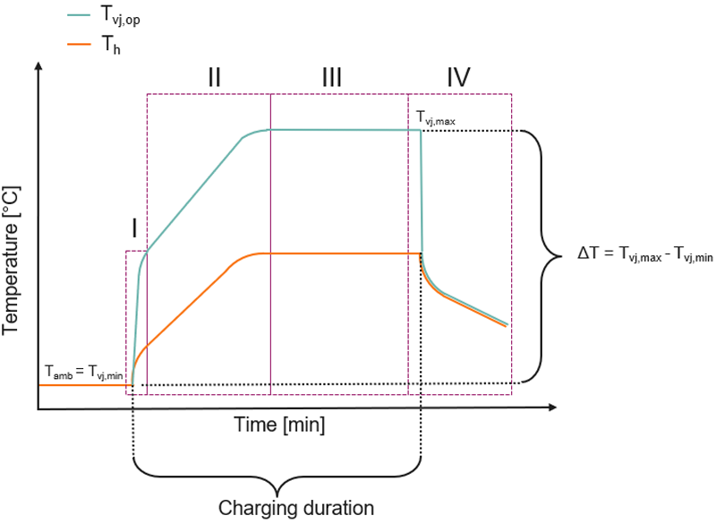
The stress caused by a charging cycle can be divided into the following (Figure 4):
1. Initiation: Initial rapid temperature rise in accordance with the thermal impedance of the module
2. Rise in temperature, influenced by the heat sink’s characteristics.
3. Attainment of steady-state temperature within the system
4. Conclusion of the charging cycle: Swift reduction in Tvj followed by continued cooling of the entire system until ambient temperature is reached or preparation for the subsequent charging cycle.
Click image to enlarge
Figure 4: Typical temperature profile during a charging cycle
The rainflow counting algorithm is a well-known approach for evaluating the fatigue of a component during a charging cycle. By implementing it in the case shown in Figure 2, the results show that the AlN-based module had 10x higher lifetime than the Al2O3-based solution. This is due to lower device temperature under the same conditions and the increased power cycling capability.
This can be a crucial part in sustainable technology development, as it directly contributes to the longevity and reliability of electronic components. By ensuring a longer lifetime of the applications, these power semiconductors can reduce the frequency of replacements and repairs. This leads to lower material consumption, reduced electronic waste, and ultimately a more sustainable approach to technology usage.


