A Better Choice for High−Speed Switching Applications

Device characterization tests and simulations on 3−phase PFC converters implemented using two different SiC MOSFETs
Figure 1: Simplified diagram of double pulse testing circuit
Silicon Carbide (SiC) has higher dielectric breakdown strength, energy bandgap, and thermal conductivity than silicon (Si), properties that power electronics designers can exploit to develop more efficient power converters with greater power density than designs based on Si IGBT devices. For these applications, minimizing conduction and switching losses at high frequencies requires devices with low RDS(on) and body diode reverse recovery charge (Qrr).
This article reviews the results of device characterization tests and simulations on 3−phase Power Factor Correction (PFC) converters implemented using two different SiC metal-oxide-semiconductor field-effect transistors (MOSFETs) in TO247−4L packages. One of the tested devices is a member of onsemi’s new EliteSiC M3S family, which is optimized for low switching losses, and the other is from a competitor, with basic parameters provided in Table 1. The article also discusses how device parameters impact their relative performance.
Understanding Power Losses
Power losses in switching devices can be categorized into conduction and switching losses. Switching losses occur because of rise and fall time, since it is not possible for current or voltage to change levels instantaneously. For power MOSFETs voltage and current, the rise and fall time are determined by how quickly a device’s parasitic capacitances are charged and discharged. Furthermore, the body diode's reverse recovery charge also contributes to the switching losses. Conversely, conduction losses occur while a device is ‘on’ conducting current. The dynamic parameters of the device determine the switching losses, while conduction losses relate to static parameters. By examining these parameters, designers can gain insight into a device’s performance relative to the magnitude of power losses. The parameters mainly responsible for switching losses are device capacitances (Coss, Ciss and Crss) and body diode reverse recovery charge(Qrr). In contrast, the significant contributors to conduction losses are RDS(on) and VSD (body diode voltage drop).
Dynamic Characterization Testing
Initially, dynamic characterization tests using a double−pulse test setup were performed under different conditions to compare the critical parameters of each MOSFET, as shown in Figure 1. Later, a 3−Phase PFC simulation was conducted to compare overall system efficiency for each MOSFET.
Click image to enlarge
Table 1: Datasheet information of the two tested devices
Comparing Static Parameters
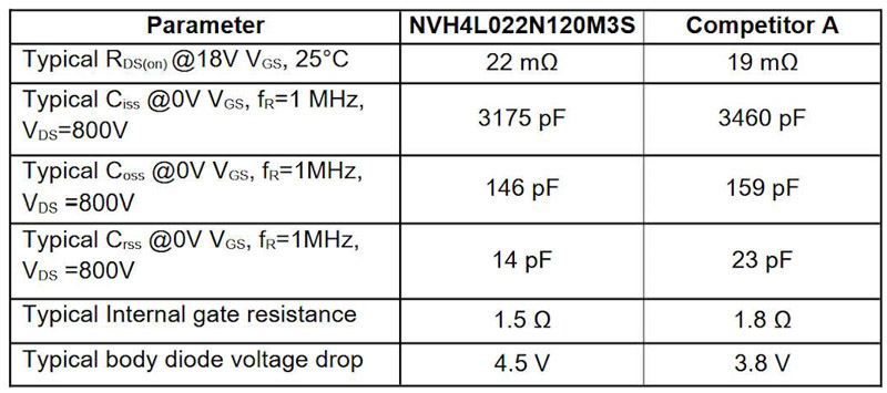
RDS(on) and VSD (body diode voltage drop) are the most critical static parameters and they were characterized under multiple test conditions. The onsemi NVH4L022N120M3S was tested against alternative SiC MOSFET from Competitor A. The results summarized in Table 2 show that onsemi’s NVH4L022N120M3S achieved superior performance with lower VSD across all measured temperatures and currents. These results will translate into lower conduction losses.
Click image to enlarge
Table 2: Comparing VSD under different test conditions
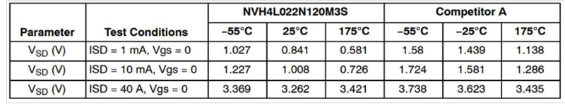
RDS(on) is another critical parameter that can be used to predict device conduction losses. Therefore, this parameter is characterized for both devices at 25°C and 175°C junction temperatures. RDS(on) measurements are performed at two gate−source voltages of 15V and 18V, using a conduction pulse width of 300µs. The results of these tests show that Competitor A has slightly lower RDS(on) for each test condition which would indicate lower conduction losses than the M3S for a given junction temperature.
Click image to enlarge
Figure 2: Comparing the RDS(on) of both MOSFETs at 25°C (left) and 175°C (right)
Dynamic Parameters
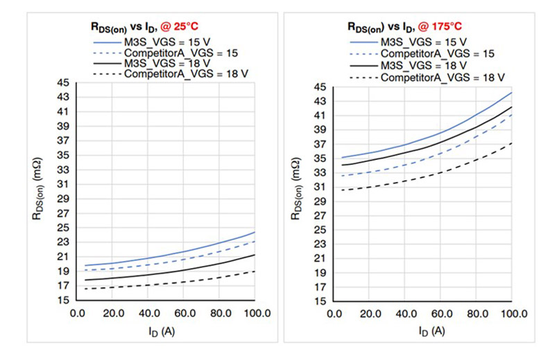
The absence of minority carriers in SiC MOSFETs means tail currents do not hinder their performance, as in Si IGBTs, and results in them having significantly reduced turn−off switching losses. Furthermore, SiC devices have a lower reverse recovery charge than Si MOSFETs, meaning smaller peak turn−on currents and lower turn−on switching loss. Input capacitance (Ciss), output capacitance (Coss), reverse transfer capacitance (Crss), and reverse recovery charge (Qrr) are the parameters which mainly contribute to switching losses, with smaller values generally resulting in lower losses. In switching applications, the drain−source voltage is significantly higher than 6V during switching transient intervals, and therefore the high voltage area is the critical portion of these switching curves. The NVH4L022N120M3S exhibits lower values for Ciss, Coss, and Crss(figure 3) when VDS ≥ 6V, meaning it has lower turn−on and turn−off losses than Competitor A.
Click image to enlarge
Figure 3: Comparing input Ciss, output Coss and reverse transfer Crss capacitances
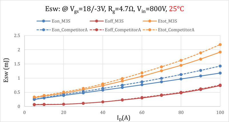
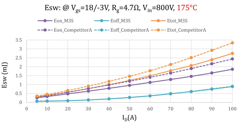
The switching energy losses for both devices are measured using double pulse testing for several load current conditions at 25°C and 175°C as shown in Figure 4 and Figure 5. The test conditions are:
l Vin = 800 V
l RG = 4.7 Ω
l VGS_on = +18 V
l VGS_off = −3 V
l ID = 5 − 100 A
On average, compared to Competitor A, the M3S exhibited 5% lower switching losses (at 25°C) and 9% lower switching losses (at 175°C) for load currents ranging from 10 A to 100 A. The main contribution comes from superior EON loss performance as a result of onsemi’s M3S process technology.
Click image to enlarge
Figure 4. Switching energy losses comparison at 25°C
Click image to enlarge
Figure 5. Switching energy losses at 175°C
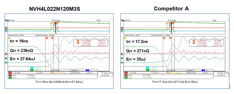
As previously mentioned, the reverse recovery behavior of a MOSFET also impacts switching losses. This parameter is tested under conditions where ID = 40 A and di/dt = 3 A/ns (with RG values adjusted for the same di/dt) at 25°C. Test results show that the M3S has a better reverse recovery performance than Competitor A due to its shorter reverse recovery time, lower reverse recovery charge, and lower reverse recovery energy.

Click image to enlarge
Figure 6: Comparison of the reverse recovery losses of M3S (left) and Competitor A (right)


Simulating MOSFET Performance
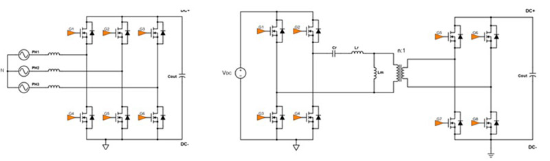
Boost-type PFC and LLC, with two inductors (LL) and a capacitor(C), are popular circuit topologies in automotive onboard chargers and HV DC/DC converters. The boost−type 3−phase PFC topology includes six switching devices, while the Full−Bridge LLC topology has four switching devices, along with a synchronous rectifier on the secondary side.
Click image to enlarge
Figure 7: Boost Type 3−Phase PFC (left) and Full−Bridge LLC (right)
Having evaluated conduction and switching losses, simulations (using PSIM) of a 3−Phase Boost−type PFC circuit were next performed to compare system efficiency using each type of MOSFET separately using the following test conditions:
l VaLL = VbLL = VcLL = 400 V
l fline = 50 Hz
l RG = 4.7Ω
l VOUT = 800 V
l fSW = 100 kHz
l POUT = 11 kW (max)
Simulation results indicate that the 3−Phase Boost PFC system using NVH4L022N120M3S exhibits higher efficiency across all operating points than Competitor A devices for the same system design.
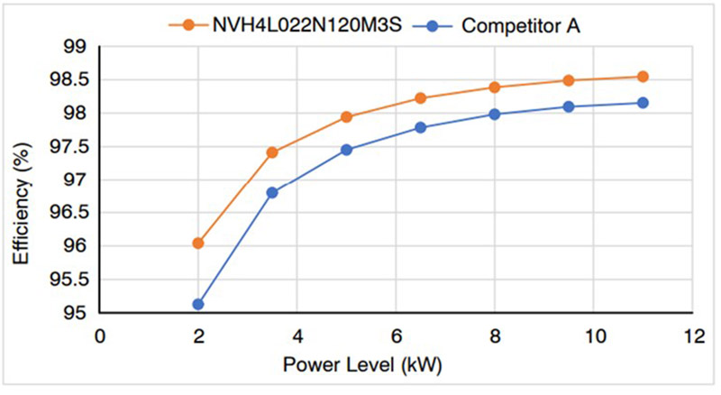
Click image to enlarge
Figure 8: Simulated estimation: Efficiency comparison at different power levels
The Better Choice
SiC devices provide several advantages over traditional Si devices in power electronics applications, including higher efficiency, lower switching and conduction losses, and the ability to operate at higher frequencies, enabling higher power density designs. Compared to a similar competing device, onsemi’s M3S technology offers superior switching performance and figures of merit, including ETOT, Qrr, VSDand overall system efficiency. M3S technology has been tailored to meet the requirements of high frequency switching applications in electric vehicles like onboard chargers and high voltage DC/DC converters. M3S MOSFETs are designed to strike an optimal balance between conduction and switching losses, making them suitable for PFC and other hard−switching applications.


