Author:
Ally Winning, European Editor, PSD
Date
09/10/2024
 PDF
PDF

Nicola Rosano, senior strategic application and system engineer, EMEA automotive at Vicor
Although we hear a lot about the undeniable benefits of GaN and SiC for power applications, there is still a lot of room for silicon to grow. Firstly, it will be many years before wide-bandgap materials can compete on cost. Silicon can also perform very efficiently. However, one of the main benefits of wide-bandgap materials is that they can switch faster with fewer losses and noise, which means that smaller magnetics can be used, enabling a more compact and power dense overall solution. Although silicon is theoretically capable of being switched a lot faster, to minimize the noise the frequency of the circuit is normally restricted, leaving designers to deal with the larger magnetics.
To try push silicon to its limits while still meeting EMC standards, Vicor decided to undertake a study. The test used the company’s NBM9280 bidirectional 400V/800V fixed-ratio conversion module in a 92 x 80mm CM-ChiP package. The module is non-regulated and non-isolated and was designed to provide a scalable onboard interface between EV batteries and roadside DC fast-charging stations. Its bidirectional capability allows it to be used for either step-up or step-down conversion.
EMC is divided in mainly in four fields; conducted emissions, radiated emissions, susceptibility to conducted emissions and susceptibility to radiated emissions. It is the former two categories that give power supplies problems and cause compliance issues, as well as other issues, including stress on components, signal distortion and reduced efficiency. Conducted emissions can be broken down into a further two areas, differential and common-mode noise, each of which has their own causes and solutions.
Nicola Rosano, who is the senior strategic application and system engineer for automotive in the EMEA region for Vicor and helped conduct the study explained, “The experiment was designed to look at the EMI challenges, and also the techniques that can be use to meet those challenges in very high-speed switching power converters. The CISPR 32 standard sets the range in which you need to be to remain compliant. Most commercial converters do not work at over 1 MHz, but typically closer to 100 kHz to stay well below the EMI conducted emission spectrum lower limit of around 125 kHz. The smart designer tends to work out at the level EMI becomes a problem and designs the circuit with that in mind. However, the consequences of using lower frequencies is that the size, the volume and the weight of the final design is higher than one that uses faster switching. So we set out to prove that Vicor parts can switch at speeds at up to 1.3 Mhz and still remain within the EMI standard range”.
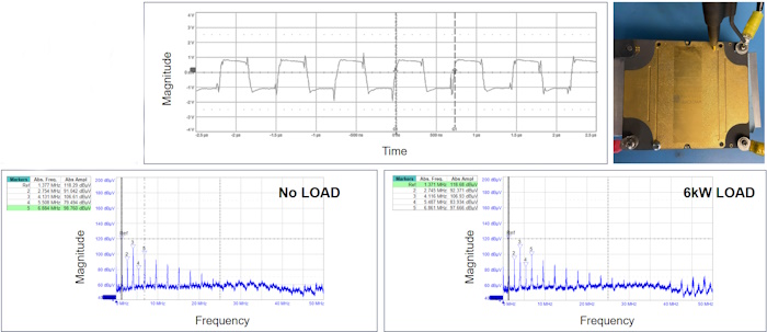
The first stage of the experiment looked at how the load affected common-mode EMI levels. It was found that the noise was relatively fixed in respect to the load (figure 2). A sniffer probe was then used to measure the harmonic content of the plating versus to the ground. The metallization characterization represents the main source of common mode noise, so it was checked initially. If the metallization is kept isolated from the power ground, the noise from the common mode component is reduced in the conducted emission test.
Figure 2; The two plots on the bottom show the frequency spectrum in two load conditions. Left has no load, and right is at a six kilowatts load. As can be seen, for this component the common-mode noise can be seen as load independent. Harmonic components have been marked up to five in the accompanying table.
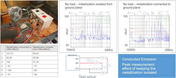
Figure 3; The results of the isolation experiment, where the CISPR 32 EMI standard limits are shown in red compared to the actual EMI results in blue
The next stage of the experiment was designed to compare the metallization when it connected to ground and when it was isolated. All of the measurements were conducted at 400V. Figure 3 shows the results, with the red lines in the two top plots identifying the quasi-peak limits of the CISPR 32 EMI standard, which represents the outer limits of the noise levels to be considered compliant, and the blue line identifies the measured noise. The two plots show the metallization connected to ground on the left, and with the metallization isolated from ground on the right. The table on the bottom left shows the measured harmonic content. Focussing on the first three harmonics, it is possible to see that the noise is substantially reduced when there is isolation between the metallization of the part and the ground plane. Future tests took that factor into account and all further results are from isolated circuits.
The next tests were taken in the time domain comparing a circuit with a bypass capacitor and one without. The 4.7nF capacitor reduced the 2Vpk-pk common mode noise to under 1Vpk-pk. If the capacitor was situated close to the high-speed voltage nodes, the common mode noise was reduced further.
The next stage of the study looked at the current distribution of the NBM9280. Rosano expands, “The scaling ratio is equal to two (400/800V) meaning theoretically the currents shown in figure 4, circled in red on the high side and the power ground should be equal. The two plots on the right identify the load current condition. When we measure the difference between the two currents, there is an offset. The yellow waveform shows the current is unbalanced, because it should have been zero while its is around 3.2 A. From an EMI point of view, the ripple of the offset is more important. Reducing this ripple will reduce the noise on the 400V side, as well as improving the overall EMI performance. Using a fluoride core that surrounds the traces in a way that the currents oppose each other has a very high impact in reducing the common-mode noise across the spectrum.”
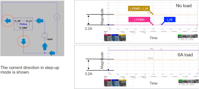
Figure 4; Theoretically the opposing currents should have cancelled each other out, leaving a small offset figure. The actual results read 3.2A
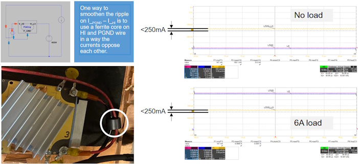
Figure 5; Splitting the current and adding a flouride core brought the current down to a more acceptable level
The final step of the study was to test the circuit with four different filter designs added. The results of the test using the optimal filter design are shown below in figure 6. The SPICE diagram on the top right of figure 6 shows a distributed common mode capacitor, and external ferrite placed on the cable, and three nested LC filters. The example confirms how even harmonics are load dependent while odd harmonics tend to be approximately similar between each other for this device.
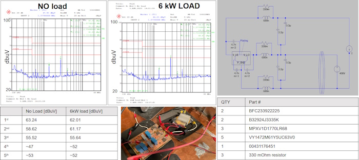
Figure 6; The results of the tests on the final circuit (top left and top centre), along with the circuit diagram (top right) BoM, (bottom right), test set up (bottom middle) and the frst five harmonic measurements (bottom right)
Conclusion
The conclusion of the experiment showed that it was possible to run the NBM9280 device at a frequencies of up to 1.3 MHz while staying within the EMI limits set by CISPR 32 by taking care in the design and implementing simple measures. High frequency implies much smaller filter components for the same power reducing the overall system volume. In addition, it has been demonstrated that obstacles on the EMI perspective can be fixed using the right design strategy. However, for automotive applications, which need to meet the limits set in CISPR 25-Class 4 & 5 would require further mitigation to reduce the second harmonic, which could possibly be achieved implementing a PI filter with a different design strategy. Alternatively a double stage filter can be used or a different type of ferrite.