Kevin Speer from Microchip tells PSD how SiC packaging needs an overhaul that focusses on removing parasitic inductance.
At any power exhibition you’ll see the ubiquitous 62mm packaging on almost any SiC manufacturer’s display. Over time, many companies have tried to improve the packaging to remove heat and for better and more reliable connectivity. However, that packaging style itself is a legacy from silicon design, and according to Kevin Speer, Director of Technology for SiC at Microchip, the industry will never get the best out of the wide bandgap material while using a package that was originally designed for silicon IGBTs.
PSD – What do you see as the main problem with SiC implementation?
KS - When people talk about silicon carbide, it is about the devices, and not many people talk about their packaging. I think the reason for that is because designing the devices, manufacturing them, and making them perform has taken many years of engineering development time. The packaging has always been an afterthought. We have just taken the silicon carbide power device and put it in the same package that silicon has used all these years.”
PSD - What type of benefits can you see new packaging bringing?
KS - Customers have other requirements than pure performance, and packaging is key to help meeting those needs. Firstly, they want efficiency and lower cost of use. Reducing the parasitic inductance of the package will achieve this and allow SiC devices to switch faster with lower switching losses.
Customers also want SiC systems to last longer. Packaging can enable this too. We can use better materials for the die attach, we can also adopt better interconnect methods - for example, using wire bonds with aluminum cladding. The copper in the core offers better thermal electrical conductivity, and you don’t need to change any tooling or equipment as it is clad with aluminum. There are other materials that can also help longevity.
The industry is currently using 3,300V SiC devices in packages that were designed for 1,200V silicon, which could shorten the device’s useful lifetime and may not have suitable creepage and clearance at that voltage. So the packaging affects performances as well as longevity.
Finally, customers want their systems to be smaller and lighter, and you achieve that through packaging by improving the way that heat is dissipated. Having lower parasitic inductance also brings the benefit of needing smaller passive components for more compact overall solutions.
PSD – So reducing parasitic losses is the main way to improve overall SiC performance?
KS - Yes, there are different types of parasitics and they affect the operation of the circuit in different ways. There is the gate-source loop, the power loop and the gate loop. In addition to that there are common paths in the circuit that are used by two different loops. Each of these loops gives rise to its own type of inductance and resulting problems.
The power loop inductance can come from the package itself and the way the board is laid out. That causes voltage overshoot when the drain voltage goes from 0V up to 600V, but it doesn't just stop there, as the parasitics cause the voltage to overshoot and then it starts to ring. The size of that overshoot is directly related to the power loop inductance. If the inductance is 2nH it can go to 620V, if it is 10nH, then it may even reach peaks of 700V. That leads to ringing at in the region of tens of MHz, which then causes EMI problems in other parts of the circuit, and, in turn, can cause the gate drivers or protection circuits to fail.
The source of the inductance in the gate loop is again the package – the length of the pins and the layout of the gate loop. Gate loop inductance causes a similar overshoot voltage, except this time it's not across the drain and source of the device, it's on the gate itself. This is a big problem as when you want the device to be off and you have ringing, the device is turned on when the voltage peaks. If you are using a half bridge topology, one of those devices needs to be off, and if not, it can cause a catastrophic failure in the circuit. Even if that doesn’t happen, the ringing will prematurely age the device.
Common source inductance can also lead to premature device failure, as well as resisting fast changes in current, so it increases switching losses. If you go from 5mH to 20mH due to parasitic common source inductance, switching loss more than double.
PSD - Do Microchip have a solution?
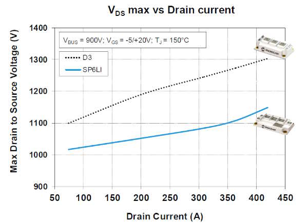
KS - Yes, in the form of the SP6LI package. For power loop inductance, the standard 62mm package has a parasitic conductance of between 15nH and 20nH and the SP6LI package is around 3nH. Figure 1 shows how that affects voltage overshoot. When you start to use the module at currents of 300A to 500A, the 62mm package reaches way over 1200 volts. So, if you're designing a system, you have to go out and buy 1700V rated module, which is more expensive, less available, and less efficient. In contrast, the SP6LI module does not come close to 1,200V, even at 450A. That allows the use of lower voltage rated devices, which are less expensive and more efficient.
Figure 1
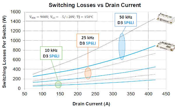
The second benefit is higher efficiency across a wide range of working conditions. In figure 2, we can see the efficiency is already better at 10 kilohertz. That gets more pronounced when the switching frequency is increased. The 62mm package has much higher losses than the SP6LI at 25kHz, and at 50KHz there is up to 40% lower switching losses. The devices inside these two packages are identical, the difference is the package.
Figure 2
Finally, reduced cost of ownership. At the 50kHz scenario in figure 2, we looked at the energy savings and converted that to an annual amount of energy. At a rate of 11 cents/kWh, the SP6LI saved over $1,000 each year. That is for one single module.


