Frederik Dostal from Analog Devices talks to PSD about how to select the correct gate driver for GaN switches for power supplies.
GaN offers a lot of benefits to designers of power supplies. Possibly the most important two of those features are GaN’s higher efficiency, and its ability to switch faster, allowing smaller magnetics to be used and therefore enabling more compact designs. However, those pluses come with one significant challenge - the gates of GaN switches are very hard to control and there is little room for error. This is because GaN’s threshold voltage for switching is very close to the over-voltage, which challenges designers to ensure the switch is fully turned on without providing a high enough voltage that could damage the switch. Different GaN suppliers also have different gate thresholds, which makes things more complex. Finally, more care has to be taken with the circuit layout.
Frederik Dostal, Subject Matter Expert, Power Management at Analog Devices explains why getting the PCB layout right is so important, “the GaN gate driver has to provide both control and protection. Careful component layout reduces the gate voltage oscillation, which can be caused by an RLC resonant tank from the parasitic gate loop inductance and resistance, and the GaN FET capacitance. We don't have to put a lot of energy into getting the gate to a voltage above the threshold, which really with the fast switching transition and to keep switching losses low. At the same time, we have to ensure that no resonant circuits are being built which would cause a false turn on. This requires a highly optimized PCB layout, more so than with silicon switches, otherwise you can have a catastrophic failure”.
GaN switches also lack a body diode, meaning that the voltage drop across the GaN FET during reverse conduction can be higher. So, while the propagation delay for the reverse recovery time is faster, when current is flowing through the reverse diode that replaces the body diode, it has a higher voltage drop. This means that dead time needs to be adjusted to make it as short as possible to stop too much energy being wasted during current flow, or while in reverse conduction mode.
Finally, in some applications, GaN switches have a higher gate leakage current. Dostal expands by saying, “If the GaN switch is operating at high frequency, there is no problem as the leakage current does not contribute to the whole power conversion efficiency too much. In some applications, such as a boost converter with both high-side and low-side GaN switches, if the input voltage gets close to the output voltage, then the high-side switch will be on for a long time. This type of circuit would have a higher leakage current, and require an energy source to keep the gate turned on for those periods.”
Analog Devices do not currently manufacture GaN devices, but the company does make controllers to drive them. In the early days of GaN, this meant adapting existing controllers and using external circuitry to protect the switch. For example, the Analog Devices LTC7800 could be used to drive GaN devices with some simple changes to the circuit design, mainly adding in diodes for protection. This could be done pretty easily with a wide variety of parts. However, the extra components made the circuit larger than it needed to be, voltage spikes could be a danger to the switches, and dead time was hard to control.
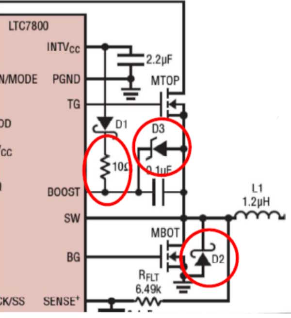
Figure 1, GaN designs can be made to work with traditional controllers, but extra protection is required.
Today’s GaN designs have continued to evolve to bring even more complex gate drive requirements, meaning a more tailored approach is often required. Dedicated gate drivers, such as Analog Devices’ LT8418 100V half-bridge GaN driver integrates both the top and bottom driver stages, along with the driver logic control and protections. It can be configured into multiple topologies and has split gate drivers to adjust the turn-on and turn-off slew rates of GaN FETs to suppress ringing and optimize EMI performance.
Dostal highlights the main benefits of the device by saying, “the LT8418 controls dead times and rise and fall times very well. The driver gets an input pulse from a controller for the high side and one for the low side. The quality of GaN drivers can be judged by the propagation delay between receiving the controller signal and outputting it to the gate. The LT8418 has a delay of 10 ns, and propagation delay matching of 1.5 nanoseconds. It also comes in a very small WLCSP package to reduce parasitic inductance, so that the gate can be driven very reliably”.
An alternative solution for smaller, more highly integrated designs would see the GaN gate drivers incorporated into the power supply controller, such as in Analog Devices’ LTC7890/LTC7891. The step-down, DC/DC switching regulator controller can drive N-channel synchronous GaN FET power stages from input voltages up to 100 V. It simplifies the design by providing a solution that has the same number of components as a traditional MOSFET design, with no need for protection diodes. The gate drive voltage can be precisely adjusted from 4 V to 5.5 V to optimize performance, and allow the use of different GaN FETs.